
Common PCB Assembly Methods and Soldering Techniques Explained
7 min
- Main PCB Assembly Methods
- Main PCB Soldering Techniques
- FAQs about PCB Assembly and Soldering
- Conclusion
Whether you're designing your first prototype or scaling up to production, understanding PCB assembly methods and soldering techniques is crucial to achieving reliable, high-performance circuit boards. Modern PCBA primarily relies on Surface Mount Technology (SMT) and Through-Hole Technology (THT)—each offering unique advantages for component density, durability, and manufacturability.
In this guide, we'll break down the major PCB assembly methods, key soldering techniques such as reflow and wave soldering, and the step-by-step PCB assembly process. You'll also learn how to identify and fix common defects like tombstoning, voids, and cold joints, helping you build cleaner, more consistent boards.
Main PCB Assembly Methods
PCB assembly is not a single technique but a collection of manufacturing strategies optimized for different component types, reliability requirements, and cost targets. The main PCB assembly approaches include Surface Mount Technology (SMT), Through-Hole Technology (THT), and mixed assembly, each with unique implications for signal integrity, thermal management, and manufacturability.
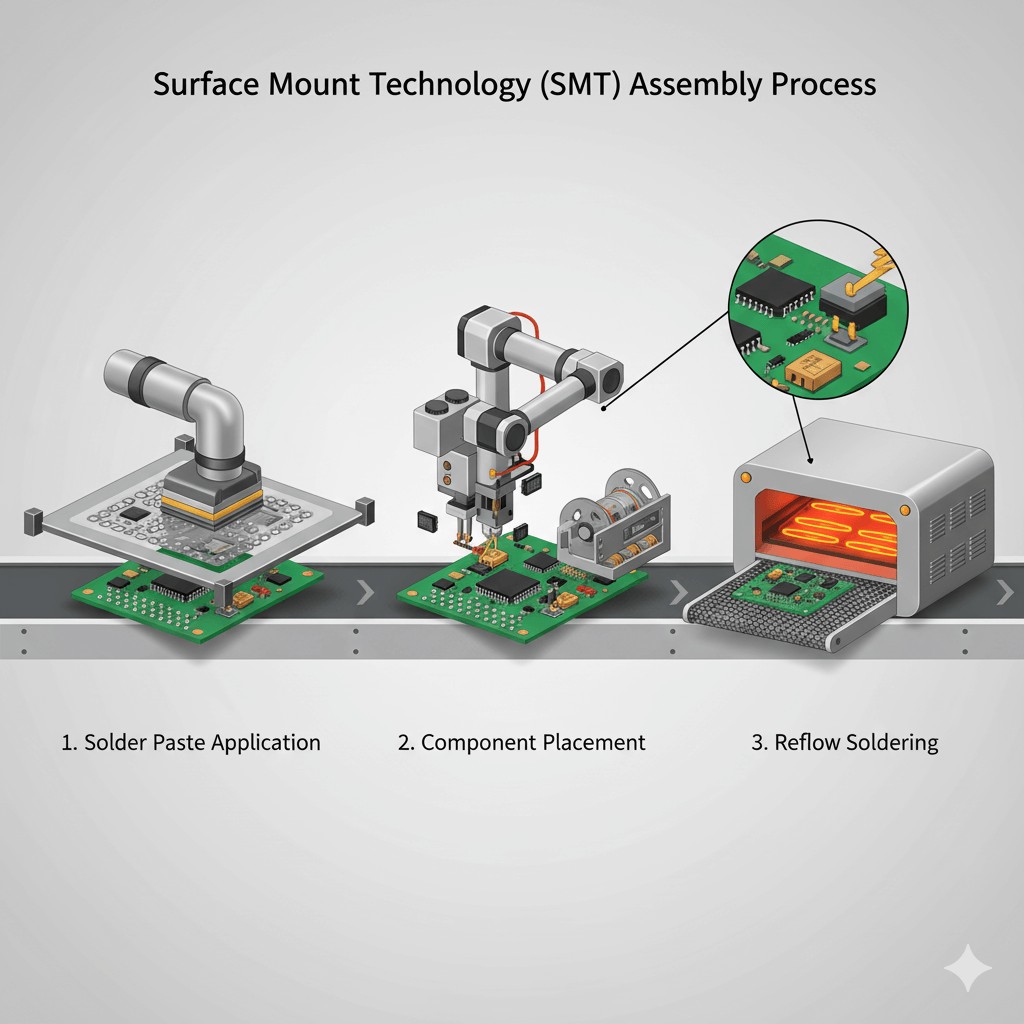
1Surface Mount Technology (SMT)
Surface Mount Technology (SMT) dominates modern PCBA because it enables miniaturization and high-density layouts. Instead of long leads, Surface Mount Device (SMD) has flat terminations or solder balls that sit directly on copper pads.
Stencil Printing
A stainless steel stencil deposits solder paste with precise volume control.
Pick-and-Place
High-speed machines place SMDs at ±25 μm accuracy.
Reflow Soldering
Thermal profile (preheat, soak, peak ~245 °C, controlled cool-down) forms intermetallic solder joints.
- From prototype builds to production runs, JLCPCB provides turnkey PCB assembly backed by automated manufacturing and a fully traceable supply chain. Upload your Gerber files and BOM, and we'll handle PCB fabrication, genuine component sourcing, precision SMT assembly, and comprehensive quality inspection—all in one streamlined workflow.
- Get an instant PCBA quote and bring your design into production today.
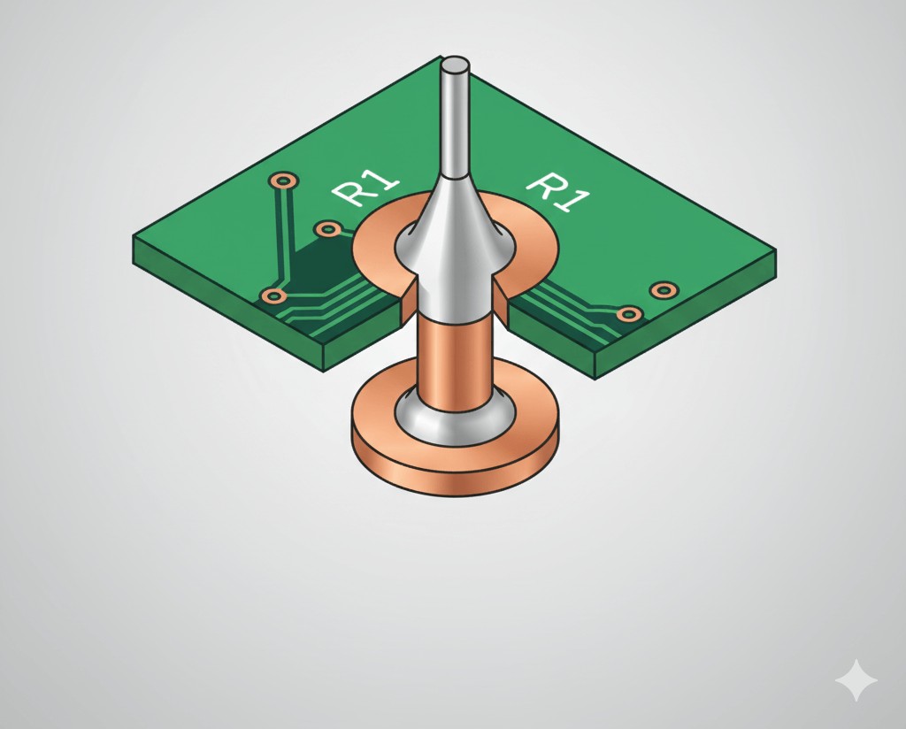
2Through-Hole Technology (THT)
Through-Hole Technology (THT) refers to the process of inserting component leads into drilled holes that are plated with copper, and then it is soldered either by wave soldering or selective soldering.
Hole Drilling
CNC drilling, plating to create conductive barrels.
Component Insertion
Manual or robotic insertion (axial or radial insertion machine).
Wave/Selective Soldering
Molten solder bonds leads to barrels.
3Mixed Assembly (SMT + THT)
Most real-world boards will use a combination of SMT and THT:
- SMT for ICs, passives, and RF circuits.
- THT for connectors, power semiconductors, and relays.
Challenges of Mixed Assembly
- Need to manage two different soldering processes (reflow + wave/selective)
- Thermal management has to address two different solder types.
- Board warpage may introduce alignment issues during the second soldering step.
To simplify this, JLCPCB offers hybrid assembly services, integrating SMT reflow and THT selective soldering.
4PCB Assembly Options: Single vs Double-Sided, Manual, and Turnkey Approaches
Single-Sided vs Double-Sided SMT: Double-sided requires more than one reflow cycle, and must be thermally balanced.
Manual Assembly: Still used for prototypes or specialized low-volume boards.
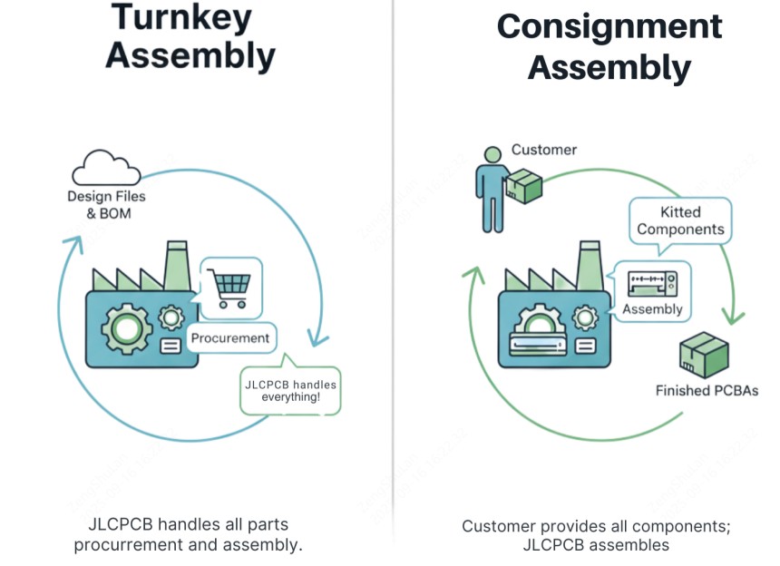
Turnkey vs Consignment PCB Assembly:
- Turnkey PCB Assembly → Manufacturer sources all parts.
- Consignment PCB Assembly → Customer supplies parts; manufacturer only assembles.
Also Read: How to Consign Parts to JLCPCB
Main PCB Soldering Techniques
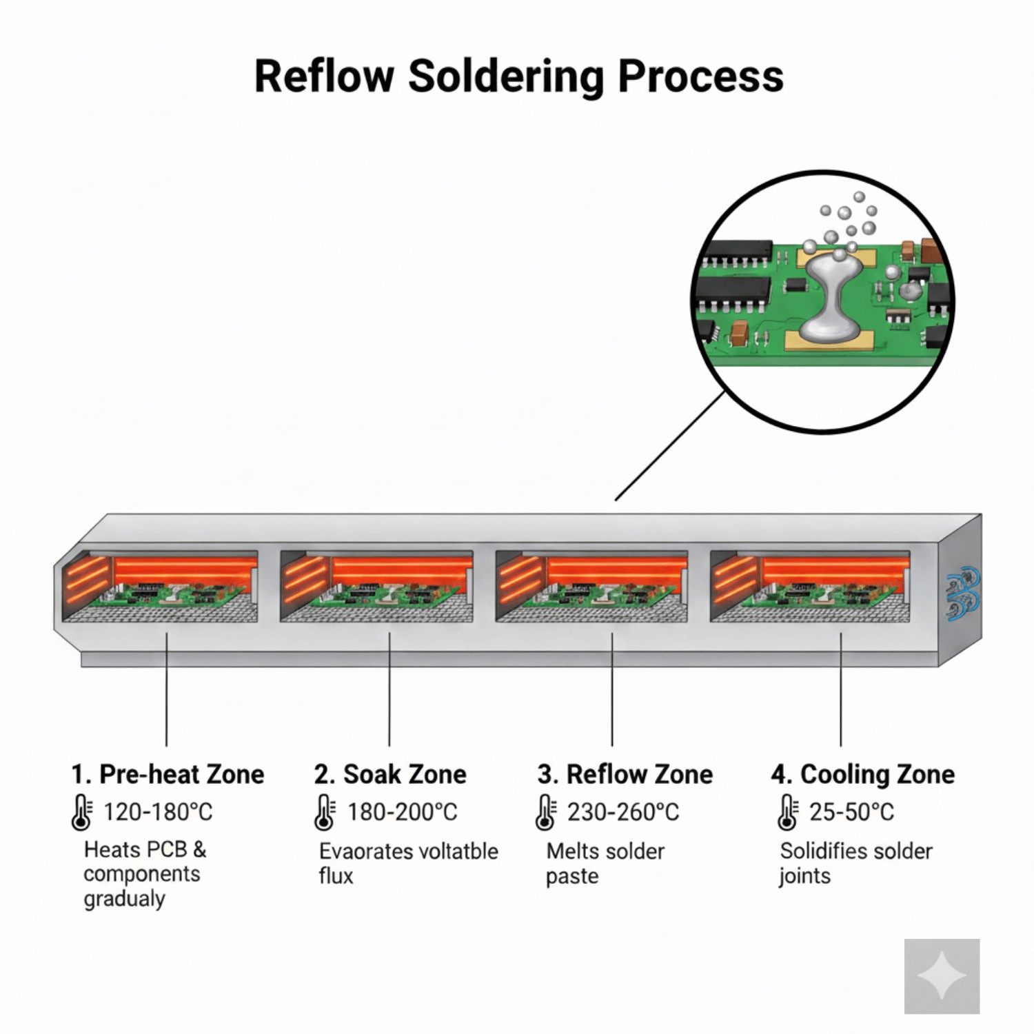
1Reflow Soldering
Reflow soldering is the primary method for soldering SMT components. The reflow soldering process includes applying solder paste via a stencil, accurately picking and placing components, and passing the assembled PCB through a reflow oven with multiple thermal zones.
A lead-free solder reflow profile, such as for SAC305 alloy, typically consists of four stages: preheat (120–150 °C), soak (150–180 °C), peak (230–250 °C), and controlled cooling. Mechanical integrity depends on proper intermetallic compound (IMC) formation, while poor thermal management can cause common reflow defects such as tombstoning, voids, or popcorning.
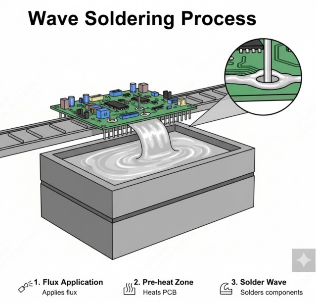
2Wave Soldering
Wave soldering is used for through-hole (THT) components and larger surface-mount (SMT) components; a PCB board is pre-fluxed and passed across molten solder (approximately 250 degrees Celsius).
Wave soldering creates strong solder joints; it is ideal for high pin-count connectors or dual-in-line package integrated circuits (DIP ICs).
Note
Wave soldering is not recommended for small/pitch SMT components or SMT components due to potential risks of bridging and thermal stresses.
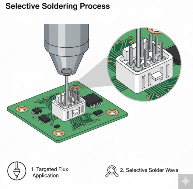
3Selective Soldering
Selective soldering applies solder in a localized area (pin) using a computer numeric controlled (CNC) soldering nozzle, which can be ideal for hybrid assemblies, i.e., an SMT component that has already been reflowed. By using selective soldering, you do not risk damaging the existing connections and minimize thermal stress on the adjacent components. Selective soldering is slower than wave soldering, but a stronger joint can be achieved.
4Hand Soldering
Manual soldering is mostly used for prototyping, rework, and low-volume boards. Hand soldering is flexible and labor-intensive, but errors can and will occur. For example, cold joints and inconsistent wetting. Hence, for high-volume productions, hand soldering should not be recommended.
FAQs about PCB Assembly and Soldering
Q: What is the difference between SMT and THT assembly?
SMT places components directly on the PCB surface using solder paste and reflow soldering, enabling miniaturization and high-density layouts. THT inserts component leads through drilled and plated holes, then solders them via wave or selective soldering for stronger mechanical bonds—ideal for connectors, power components, and high-reliability applications.
Q: What is the most common soldering method for SMT components?
Reflow soldering is the primary method for SMT components. It involves applying solder paste via a stencil, placing components, and passing the PCB through a reflow oven with controlled thermal zones (preheat, soak, peak ~245 °C, cooling) to form reliable intermetallic solder joints.
Q: Can SMT and THT be used on the same PCB?
Yes, this is called mixed assembly. SMT components are placed and reflowed first, then THT components are inserted and soldered via wave or selective soldering. Challenges include managing two different soldering processes and potential board warpage during the second soldering step.
Q: What is the difference between turnkey and consignment PCB assembly?
In turnkey assembly, the manufacturer sources all components and handles the entire process. In consignment assembly, the customer supplies the parts and the manufacturer only performs the assembly. Turnkey reduces procurement burden, while consignment gives the customer more control over component sourcing.
Q: What are common PCB assembly defects and how can they be prevented?
Common defects include tombstoning (uneven solder wetting causing components to stand up), voids (trapped gas in solder joints), cold joints (insufficient heat/dull appearance), and bridging (unintended solder connections between pins). Prevention requires proper stencil design, optimized thermal profiles, controlled cooling rates, and thorough inspection using AOI or X-ray.
Conclusion
Mastering PCB assembly is about precision, consistency, and quality control—from selecting the right assembly method (SMT, THT, or mixed) to applying the proper soldering technique for each component type. Understanding how to prevent and fix assembly defects not only improves circuit board reliability but also reduces production waste and rework.
Popular Articles
• Common PCB Assembly Methods and Soldering Techniques Explained
• What Is BGA Void? Causes, IPC Limits, and Solutions
• SMD Soldering Tools You Need: Complete Guide from Beginner to Pro
• Reflow Soldering: Everything You Need to Know
• SMT Assembly Process Explained and Equipment Used: A Step-by-Step Guide to PCBA Manufacturing
Keep Learning
Common PCB Assembly Methods and Soldering Techniques Explained
Whether you're designing your first prototype or scaling up to production, understanding PCB assembly methods and soldering techniques is crucial to achieving reliable, high-performance circuit boards. Modern PCBA primarily relies on Surface Mount Technology (SMT) and Through-Hole Technology (THT)—each offering unique advantages for component density, durability, and manufacturability. In this guide, we'll break down the major PCB assembly methods, key soldering techniques such as reflow and wave sold......
12 Professional Soldering Tips and Tricks Every Beginner Should Know
Soldering is not merely "gluing" metal; it is a metallurgical process that creates an intermetallic compound (IMC). This molecular bond ensures the electrical and mechanical integrity of your device. A poor joint might pass a quick visual check but will inevitably fail under vibration or thermal stress, leading to "ghost" bugs and hardware failures. These soldering tips and tricks focus on practical, repeatable techniques used in professional electronics soldering—from correct heat transfer and flux u......
Solder Melting Point Guide: Chart, Alloy Types, and Reflow Considerations
In the precise world of electronics manufacturing, a difference of just a few degrees can mean the distinction between a perfect, reliable solder joint and a catastrophic "cold" joint failure. While many hobbyists view soldering simply as "melting metal to stick things together," professional PCB assembly requires a nuanced understanding of thermodynamics. The solder melting point is not simply a single value listed in a datasheet; it is a decisive limit that determines the choice of components, the s......
The Ultimate Guide to Solder Flux: Everything You Should Know Before Soldering PCB
Soldering is needed to make almost all electronic devices. Adding solder alone won't make a joint that is strong, clean, and sound from a metallurgical point of view. Solder flux is a very important part of the process that comes in here. If you want to do your job better and make it more reliable, you need to know a lot about soldering flux, whether you're an engineer, a professional technician, or just a hobbyist. This article goes into a lot of detail about solder flux, including what it is, how it......
Flex PCB Assembly Guide: Process, Challenges, and Solutions
Flexible Printed Circuit Boards (Flex PCBs) are the foundational technology enabling the compact, innovative design of modern electronics. Because of their ability to bend and fold, they power devices from smart wearables to compact medical instruments where traditional rigid printed circuit boards (Rigid PCBs) can't be used. Achieving a functional electronic circuit from the raw plastic film demands special expertise, with flexible PCB assembly (FPCA) representing the crucial final step in this trans......
SMD Rework Guide: Tools, Temperatures, and Techniques That Prevent PCB Damage
From replacing a burned regulator to correcting wrong component values or removing solder bridges on fine-pitch ICs, SMD rework is an essential skill in electronics manufacturing and prototyping. It allows engineers to repair assembly defects, implement design changes, and recover valuable PCBs without the cost and delay of building new boards. In this guide, you will learn: What SMD rework is Common rework scenarios Tools and temperatures Safe removal and installation Package-specific techniques Real......