
Mastering Mitered Corners for Superior High-Speed Signal Performance
15 min
- Why Mitered Corners Are Essential in High-Speed PCB Design
- Core Design Rules for Effective Mitered Corners
- Common Pitfalls and How to Avoid Them
- Precision Manufacturing of Mitered Corner PCBs
- JLCPCB's Expertise in Delivering Flawless Mitered Corner PCBs
- Frequently Asked Questions (FAQ)
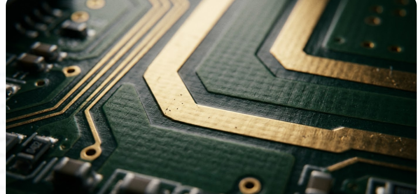
Have you ever had the privilege of zooming into a PCB layout and noted those well-chamfered corners on high-speed signal traces? Mitered corners they are, and much more than a cosmetic preference. The geometry of each trace bend is directly proportional to impedance continuity, signal reflection, and the quality of your data being transmitted at the RF and high-speed digital frequencies. Having mitered corners on your PCB can be the difference between meeting your return loss target and trying to trace the cause of the elusive signal integrity breakage in your board with numerous board spins.
The manner in which you address direction change is important, whether you are routing a 10 GHz RF feed network, a multi-gigabit SerDes lane, or a millimeter-wave antenna trace. Acute 90-degree angles form local impedance discontinuities, which reflect energy back to the source. These reflections are inconsequential at lower speeds. However, with the edge rates becoming sharp and an increase in carrier frequency, that little corner discontinuity begins to appear in your S-parameter plots and eye diagrams.
This day, we will take a tour of what goes into mitered corners, why and when they are important, how to size them properly, and how to prevent the pitfalls many designers and manufacturers fall into because they have not understood the engineering behind them. We shall also discuss the choice of mitered and curved bends, combining with differential pairs, and the fabrication controls required to get your desired geometry onto the finished board. Let's get into it.
Why Mitered Corners Are Essential in High-Speed PCB Design
The Signal Reflection Problem at Sharp 90-Degree Corners
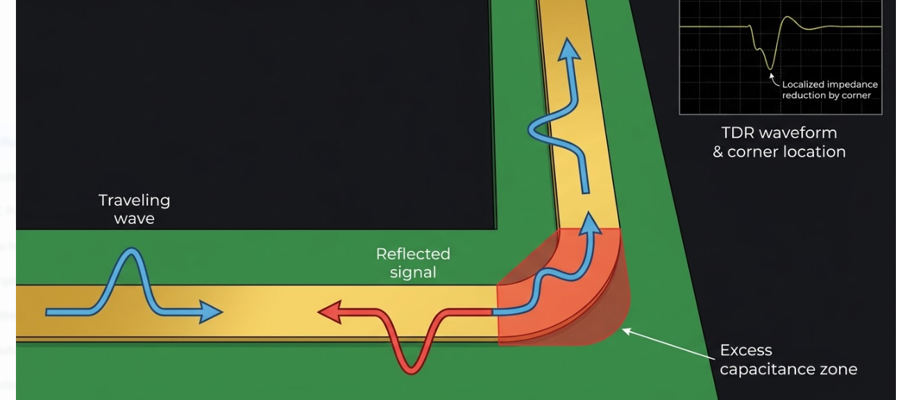
As a trace of microstrip or stripline approaches a sharp 90-degree turn, the effective width of the conductor becomes larger at the corner. The intersection point of the horizontal and the vertical segment forms a little patch of the additional copper, which is larger than the nominal trace width. This additional copper adds the local capacitance to the reference plane, causing an impedance discontinuity. There is a momentary dip in the impedance at the corner, and any change in the impedance along a transmission line will result in part of the signal energy being reflected back to the source.
This reflection is dependent on the frequency and edge rate. With frequencies less than approximately 1 GHz or with rise times of digital signals less than about 1 ns, the corner discontinuity electrical length is a minute fraction of a wavelength. The reflection lies within the noise floor and does not have any viable effect on signal quality.
The scenario is far different when you get to RF and microwave frequencies, or when you have to contend with multi-gigabit digital signals with edge rates less than 100 ps. A wavelength of FR4 microstrip is approximately 16-17 mm at 10 GHz. The corner region is a physically small part, but an electrically significant fraction of that wavelength. Reflections summed at several bends in a signal path cause accumulated reflections and reduce return loss as well as distort the signal waveform.
How Mitered Corners Improve Impedance Continuity
Mitering eliminates the copper on the outer side of the corner and the redundant material that gives rise to the capacitive discontinuity. The chamfering of the corner at a 45-degree angle decreases the effective width of the conductor at the bend, returning the continuity of impedance due to the direction change.
The extent of copper excision is expressed as the miter percentage, which refers to the amount of corner diagonal excised. An ideal miter usually eliminates 60-70 percent of the corner area with most practical geometries of microstrip. This value is not arbitrary. It is a result of the literature of microwave engineering, which means the amount of copper one must remove to offset the additional capacitance at the bend without over-correcting.
Core Design Rules for Effective Mitered Corners
Optimal Miter Angle and Length Guidelines
Designing effective mitered corners is not a matter of applying a single rule universally. It requires a structured workflow that considers your specific impedance targets, stackup, and frequency range. Here is the recommended design approach:
- Define target impedance: Establish the characteristic impedance for each controlled net class (e.g., 50 ohm single-ended, 100 ohm differential).
- Lock the stackup: Confirm dielectric thicknesses, Dk values, and copper weights with your fabricator. The miter geometry is only valid for a specific cross-section.
- Calculate the baseline miter: Use the established microwave formula for optimal miter percentage. The widely referenced Douville and James approximation gives the optimal miter fraction as M = (52 + 65 * exp(-1.35 * (W/H))) percent, where W is trace width and H is dielectric height.
- Simulate the bend: Run a 2.5D or 3D electromagnetic simulation of the actual bend geometry on your stackup to verify S-parameters meet your targets.
- Lock geometry in routing rules: Once validated, encode the miter dimensions into your EDA tool's design rules so every bend is applied consistently.
The limits of validity of formula-based approximations are worth mentioning. Classical miter equations were formulated in the case of microstrip lines having a W/H ratio of about 0.5 to 2.0. Beyond this range, especially in very narrow or very wide traces compared to the dielectric height, the formulas are less accurate, and EM simulation is required.
| W/H Ratio | Miter Percentage (Approximate) | Formula Reliability | Recommendation |
| 0.5 - 1.0 | 55 - 65% | Good | Use the formula as the starting point, and verify with a simulation |
| 1.0 - 2.0 | 65 - 75% | Good | The formula is generally reliable |
| Below 0.5 | Varies | Poor | EM simulation required |
| Above 2.0 | Varies | Moderate | EM simulation recommended |
When to Use Mitered vs. Rounded Corners
One of the questions that re-emerges with high-speed and RF PCB design is the decision between mitered bends and rounded (arc) bends. There is no universal superiority of the two. The correct decision will be based on frequency, routing density, and manufacturing constraints.
Here is a practical decision matrix:
- Mitered bends: Offer compact direction changes with near-rounded performance when properly tuned. They are the workhorse solution for most high-speed digital and RF designs below 10-15 GHz.
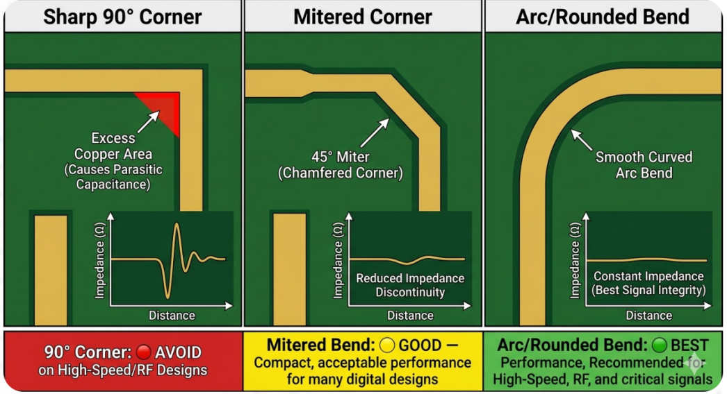
- Sharp 90-degree bends: Should be avoided on any critical RF or high-speed net. They are acceptable only on low-frequency, non-impedance-controlled signals where the reflection is inconsequential.
Recent layout software, such as EasyEDA, Altium Designer, and KiCad, can now perform accurate arc routing and can quickly compare S-parameter results between bend choices. Assuming that your tool has arc routing and that your board density allows it, then there is no reason not to arc the most important RF nets. All other cases are best served with a well-sized miter offering better routing overhead.
Integration with Differential Pairs and High-Frequency Traces
Differential pairs are more difficult to deal with at bends since it is as important to preserve the symmetry of the pairs by reversing the direction of each trace as it is to deal with the impedance of each trace. The inner trace takes a shorter path when a differential pair rounds a corner than the outer trace. This difference in path length also adds skew, converts the differential signal energy into common-mode noise, and reduces the noise rejection capability of the pair.
The key rules for bending differential pairs are:
1.Match electrical length: Both traces in the pair must have the same electrical length through the bend. If mitering, apply identical miter geometry to both traces and compensate for the path difference using serpentine tuning on the shorter (inner) trace.
2.Maintain consistent spacing: Keep the differential pair gap constant through the bend. Allowing the spacing to vary changes the differential impedance.
3.Preserve reference-plane continuity: The ground or power plane beneath the differential pair must remain solid and uninterrupted through the bend zone. Any slot or void in the reference plane disrupts the return current path and increases common-mode radiation.
4.Consider via-fencing at bends: For critical RF differential pairs, placing ground stitching vias along the outside of bends helps contain the electromagnetic field and suppress substrate modes.
Common Pitfalls and How to Avoid Them
Over-Mitering or Under-Mitering Issues
A mistake in the miter percentage in either direction has some very specific failure modes, and both are actually very common in production designs.
Under-mitering is a situation where there is a removal of less copper than is required. The remaining excess capacitance is left behind, and although the discontinuity is smaller than that in a sharp 90 bend, it produces measurable reflections at high frequencies. The corner impedance dip remains and is manifested as a localized capacitive blip on a TDR trace. In the case of a single bend, the effect can be minimal. However, on a path with many bends, the effect may go cumulative, putting return loss out of specification.
The other issue is over-mitering, which is possibly more destructive. In case of excess removal of copper, the trace cross-section in the corner is reduced to less than the nominal width. This produces an inductive impedance spike (impedance increase) on the bend, and the narrowed conductor also focuses current density, producing localized current crowding. This current crowding may cause reliability problems at high power levels or in designs with tight thermal margins.
Manufacturing Tolerances That Affect Corner Accuracy
The most carefully designed miter may lose its usefulness when manufacturing tolerances change the achieved geometry to values different from what was intended in the design. A number of variables of fabrication directly influence corner accuracy:
- Etch tolerance: Standard PCB fabrication has an etch width tolerance of plus-or-minus 0.3-5 mil (13-25 um). A 1-mil trace etch difference is a 20 percent width change on a 5-mil-wide trace, which is a substantial change in impedance. In the narrowed geometry at the miter point, the percentage effect of this tolerance is even greater.
- Dielectric thickness tolerance: Prepreg and core thicknesses vary by plus or minus 10% in standard processes. Since impedance depends on the dielectric height, this variation compounds with etch tolerance to widen the impedance distribution.
- Registration accuracy: Layer-to-layer registration ensures that the trace on the signal layer aligns correctly with the reference plane beneath it. Misregistration shifts the effective trace-to-plane geometry and can alter impedance by 1-3 ohms on tight designs.
Precision Manufacturing of Mitered Corner PCBs
Advanced Etching and Registration Control for Sharp Corners
The mitered corner you have created in your EDA tool is as good as the process that has created it on copper by reproduction. Etch control and layer registration are two manufacturing controls that are of particular importance with respect to maintaining desired bend geometry.
Etch control defines the accuracy with which the trace profile is a replica of the Gerber artwork. The tightly controlled etch chemistry and conveyor speed are used by modern PCB fabricators to reduce the undercut variation. Where the copper feature can be tapered to a point, such as fine-geometry features, such as miter tips, it is crucial that etch uniformity is achieved across the panel. Unetched panels result in varying miter geometry between boards causing a direct relationship between varying impedance at the bends.
Quality Assurance to Verify Miter Accuracy and Signal Integrity
A robust quality assurance flow for mitered corner PCBs follows a three-stage verification process:
1.Geometry check: On etching, verify that the miter dimensions are within tolerance with the artwork. AOI systems match the etched copper features to the Gerber reference and indicate any dimensional variation. In critical designs, cross-section analysis is used to give a specific trace width, copper thickness, and dielectric height at the bend point.
2.Impedance coupon and TDR measurement: Incorporate impedance test coupons on the production panel to duplicate the geometry of the controlled impedance trace with representative bends. Use a TDR device to measure these coupons and ensure that the characteristic impedance does not go out of the tolerance window (e.g., 50 ohm and 10 percent). An effective coupon scheme will identify process drift before completed boards are dispatched.
3.Signal integrity acceptance criteria: Establish pass/fail levels that are significant to your application. Typical requirements are impedance within the desired tolerance range, -15 dB (or -20 dB in more demanding RF designs) return loss over the operating bandwidth, and less than the link budget insertion loss.
| QA Stage | Method | Typical Acceptance Criteria |
| Geometry | AOI, cross-section | Trace width within plus or minus 0.5-1.0 mil of artwork |
| Impedance | TDR coupon measurement | Plus or minus 10% of target (standard), plus or minus 7% (tight) |
| Return loss | VNA measurement (if specified) | Better than -15 dB across the operating band |
| Insertion loss | VNA measurement (if specified) | Within the allocated link budget |
Scaling from Prototypes to High-Volume Production
A key issue that has been ignored in high-speed PCB manufacturing is ensuring that your performance remains consistent when you are moving out of prototype quantities to volume production. The only thing that is useful about a prototype board is that it has to be able to be scaled to achieve the same impedance and signal integrity requirements.
- Same stackup family: Use the same prepreg types, core materials, copper weights, and lamination sequence in production as in the prototype. Any material substitution, even a different prepreg weave style with the same nominal thickness, can shift Dk and alter impedance.
- Same fabrication notes: The fab drawing, stackup specification, impedance callouts, and special instructions that produced a successful prototype must transfer identically to the volume production order.
- Same coupon design: The impedance test coupons used for prototype validation should be the same coupons used for ongoing production monitoring. Changing the coupon geometry between prototype and production introduces a measurement variable that obscures process changes.
JLCPCB's Expertise in Delivering Flawless Mitered Corner PCBs
State-of-the-Art Equipment for Precise Trace Geometry
Precision mitered corner designs demand a fabricator with tight process control over trace geometry, and this is where JLCPCB's manufacturing capabilities align well with high-speed design requirements. Their impedance-controlled PCB service supports fine trace and space geometries that are essential for accurate miter reproduction.
Key capabilities relevant to mitered corner PCBs include:
- Minimum trace/space: Down to 3.5/3.5 mil for standard impedance-controlled designs, enabling fine-pitch routing with accurate miter geometry.
- Controlled-impedance tolerance: Standard plus or minus 10%, ensuring that the impedance continuity you designed at the mitered corners is maintained in production.
- Layer support: Impedance-controlled stackups from 4-layer through complex multilayer configurations, with defined dielectric materials and thicknesses.
- TDR verification: Every impedance-controlled order includes a coupon-based TDR measurement to confirm that the manufactured board meets the specified impedance target.
These manufacturing parameters directly support the kind of precision needed for well-executed mitered corners. When your design calls for a miter tip that tapers to a specific width, tight etch control and fine trace capability ensure the fabricated geometry faithfully reproduces your design intent.
Integrated DFM Feedback for Optimal High-Speed Results
Bend geometry review: Ask the fabricator to confirm that the miter dimensions at each bend point are within their etch capability. Very aggressive miter tips that taper to extremely narrow points may be clipped by the etch process.
Impedance structure verification: Confirm that the stackup, trace width, and dielectric values in the impedance calculator match what will actually be built. JLCPCB's online impedance calculator references their real production stackups, so the Dk values and layer thicknesses correspond to actual factory materials.
The DFM review procedure of JLCPCB compares Gerber files uploaded to manufacturing capabilities and points out certain difficulties that can be encountered prior to the commencement of production. In the case of impedance-controlled boards, this involves ensuring that trace widths and the corresponding stackup are compatible with the desired impedance levels. PCBs costing only 2 dollars and impedance-controlled options costing only slightly more, high-speed proof of designs in prototype and production is affordable and practical.
Frequently Asked Questions (FAQ)
Q1: What is the difference between a mitered bend and an arc bend on a PCB trace?
A mitered bend chamfers the outside corner of a 90-degree trace bend at a 45-degree angle, removing excess copper to reduce the capacitive discontinuity. An arc bend replaces the sharp corner with a smooth curved radius, distributing the direction change over a longer path.
Q2: When is a 90-degree corner actually acceptable on a PCB trace?
Sharp 90-degree corners are acceptable on non-impedance-controlled signals operating well below 1 GHz, such as slow GPIO lines, low-frequency analog signals, or power distribution traces. They are also a non-issue on traces where the signal bandwidth is low enough that the corner's electrical length is negligible.
Q3: How do I calculate the correct miter size for my trace geometry?
Start with the Douville and James approximation: Miter percentage M = (52 + 65 * exp(-1.35 * (W/H))) percent, where W is trace width, and H is dielectric height. This gives a good baseline for W/H ratios between 0.5 and 2.0.
Q4: How should I handle mitered corners on differential pairs?
Apply identical miter geometry to both traces in the pair. Maintain constant spacing between the two traces through the bend to preserve differential impedance. Compensate for the path-length difference between the inner and outer traces using serpentine tuning on the shorter trace.
Q5: What manufacturing tolerances affect mitered corner performance?
Three main tolerances affect miter accuracy. Etch width tolerance (typically plus or minus 0.5-1.0 mil) changes the realized trace and miter dimensions. Dielectric thickness tolerance (plus or minus 10% standard) alters impedance through the dielectric height parameter.
Keep Learning
Your Ultimate Guide to PCB Rulers
In the world of PCB design and manufacturing, having the right tools is crucial for achieving accuracy and precision. One such tool that has gained popularity among professionals and hobbyists is the PCB ruler. This specialized measuring tool is designed to provide accurate measurements, reference information, and component footprints, assisting designers, engineers, technicians, and assemblers in various stages of PCB development. In this guide, we'll explore what a PCB ruler is, the features and mea......
Understanding the Materials Used in PCBs: Selection, Types, and Importance
Key Takeaways FR-4 is the go-to material for most cost-effective and reliable PCBs. Use Rogers for high-frequency and RF applications to reduce signal loss. Higher copper weight (2oz) improves current and heat handling. Choose High-Tg substrates for better thermal stability in multilayer boards. Green LPI soldermask offers the best balance of performance and inspection. Printed circuit boards (PCBs) are an essential component of modern electronics. These boards connect and support electronic component......
How to Select Tg of PCB ?
What is the Tg of PCB? In PCB manufacturing, "Tg" stands for Glass Transition Temperature. It is the temperature at which the PCB substrate material transitions from a rigid, glassy state to a soft, rubbery state. PCBs are flame-retardant (UL94 V-0) and do not burn easily; instead, they soften above Tg. The Critical Correlation Between Tg and Z-Axis CTE (Coefficient of Thermal Expansion) When the temperature exceeds the Tg point, the PCB substrate material (such as standard FR-4) undergoes a physical ......
How to Choose the Thickness of PCB
First, In the world of electronic products, the PCB is often referred to as the "heart" of the device. It interconnects all components, making board thickness one of the most important parameters. Choosing the right PCB thickness directly affects the electrical performance, mechanical stability, thermal management, and long-term reliability of the final electronic product. The process of selecting PCB thickness is influenced by various factors, such as product application scenarios, board material, an......
PCB Copper Pour Basics
What is Copper Pour in PCB Design? Copper pour refers to the technique of filling unused areas of a PCB's copper layers with solid copper planes. These planes are connected to power or ground nets, creating a continuous conductive path. Copper pour is typically used in the power and ground planes, as well as in signal layers for specific purposes. Purpose and Benefits of Copper Pour: Copper pour is primarily used to fill unused areas on PCB copper layers with solid (or hatched) copper connected to pow......
How to Prevent Solder Bridges for Superior PCB Quality and Reliability
Key Takeaways Solder bridges are a leading cause of SMT failures on fine-pitch components. Prevent them with proper solder mask dams (0.075–0.1mm), optimized stencil design, and controlled reflow profiles. Combine good DFM practices with AOI + X-ray inspection for maximum reliability. Professional manufacturing and early DFM review significantly boost first-pass yield and reduce costly rework. You have experienced the post-reflow sadness and eyed the board that failed on the first reflow, if you have ......