Demystifying PCB Trace Length Matching vs Frequency: Ultimate Guide
13 min
- Introduction
- The Relationship Between PCB Trace Length Matching and Frequency
- What Really Determines Length Matching Requirements
- Differential Pair Length Matching Tolerance: How Much Skew Is Acceptable?
- Comparative Guide: Serpentine vs. Sawtooth Length Matching
- Reference Table: High-Speed Interface Length Matching Recommendations
- FAQ about PCB Trace Length Matching vs Frequency
Key Takeaways
- Signal rise time, not clock frequency, is the true determinant of trace length matching tolerance.
- A 10 MHz clock with a 100 ps rise time behaves like a GHz signal and demands strict matching.
- Dielectric dispersion causes phase velocity to shift across the spectrum, invalidating single-frequency matching assumptions.
- Designers should match by time-domain delay in picoseconds, not by physical length in mils.
- Serpentine routing suits single-ended traces, while sawtooth tuning preserves coupling in differential pairs.
Introduction
PCB designers have relied on length matching in pcb for years. Route traces of equal length, the thinking goes, and the signals arrive together. This idea rests on false premises that cost engineers debug hours and full board respins. Length matching aligns propagation delays across parallel paths to prevent skew. In a source-synchronous bus, data lines must arrive within a fraction of the clock period. In a differential pair, both halves must arrive simultaneously, or the signal degrades into common-mode noise. A common topic of confusion is PCB trace length matching vs frequency, and whether frequency truly dictates design constraints.
The Relationship Between PCB Trace Length Matching and Frequency
The question this guide addresses is straightforward: does frequency actually dictate the matching rules?
The First Misconception: Equal Length Equals Equal Arrival
Equal physical length does not guarantee simultaneous arrival. Even if two traces measure identically in mils, several factors desynchronize them:
- Layer transitions. Different routing layers expose signals to different dielectric environments. A microstrip trace on the outer layer propagates faster than a stripline buried in the core, because part of a microstrip's field travels through air.
- Via structures. Via transitions introduce parasitic capacitance and inductance that alter the effective propagation velocity and add delay that pure length calculations ignore.
- Dielectric constant variation. The dielectric constant (Dk) of the laminate varies across a board and even within a single trace path, because of resin-to-glass ratio changes, causing local velocity shifts.
- Copper roughness and skin effect. At higher frequencies, current crowds toward the rough copper surface, lengthening the effective current path and distorting the propagation constant.
Equal length does not equal equal delay. The mils on your CAD ruler are a proxy for delay, and a leaky one at that.
The Second Misconception: Higher Clock Speed Demands Stricter Matching
It is tempting to believe that a 4 GHz processor bus requires tighter length matching than a 100 MHz microcontroller. This intuition conflates clock frequency with the signal bandwidth that actually matters.
A digital square wave is not a single tone. It is the sum of a fundamental and a theoretically infinite series of odd harmonics. What defines the highest meaningful harmonic is not the clock rate but the sharpness of the edges. A 10 MHz clock with a very fast 100 ps rise time contains significant frequency content up to roughly 5 GHz (via the knee-frequency approximation fknee≈0.5/tr) . That "slow" 10 MHz clock therefore demands the same length matching discipline as a 5 GHz signal.
Conversely, a 200 MHz clock generated with deliberately slow, filtered 2 ns edges has a knee frequency near 250 MHz and tolerates far looser matching than its clock rate would suggest.
The True Rule: Rise Time Rules Everything
The principle that resolves the confusion is this: signal rise time determines trace length matching tolerance. The edge rate sets the effective bandwidth, and it is bandwidth, not the carrier frequency, that governs how tightly you must match.
This reframes the entire approach to high-speed layout. Instead of asking what frequency am I running, the disciplined designer asks how fast is my signal edge and what bandwidth does that imply. Everything downstream, skew budgets, tuning strategy, layer assignment, flows from that single question.
What Really Determines Length Matching Requirements
Digital pulses are broadband. Their energy spans from DC to well beyond the knee frequency set by the rise time. This broadband nature is exactly why "matching at a frequency" is ambiguous. A single matching frequency captures only one slice of a signal that lives across many decades of the spectrum.
To match correctly, you must understand how the transmission medium behaves as a function of frequency, not as a fixed constant. Three phenomena dominate: dielectric dispersion, frequency-dependent loss, and the relationship between rise time and knee frequency.
Dielectric Dispersion and Phase Velocity Changes at High Frequencies
The dielectric constant (Dk) of a PCB substrate, whether standard FR-4 or a high-speed laminate such as Megtron 6 or Rogers material, is not a fixed number. It decreases gradually with frequency, a phenomenon known as dielectric dispersion. Because propagation velocity is tied directly to the effective dielectric constant, dispersion means the signal's speed changes with frequency:

where c is the speed of light and epsilon_eff is the effective dielectric constant seen by the trace, a quantity that is itself frequency-dependent.
The consequence is subtle but critical. The low-frequency components of an edge travel at a slightly different speed than the high-frequency components. This spreads the edge in time and means that a length match valid at 1 GHz is not necessarily valid at 10 GHz.
Simulated data comparing materials shows significant phase velocity differences; for example, the actual change in Dk of standard FR-4 from 1 MHz to 20 GHz (approximately 4.7 down to 3.8) results in a phase velocity change of roughly 1.11x. Advanced materials like Rogers 4350B or Megtron 6 exhibit far less dispersion, keeping speeds much more consistent across frequencies.
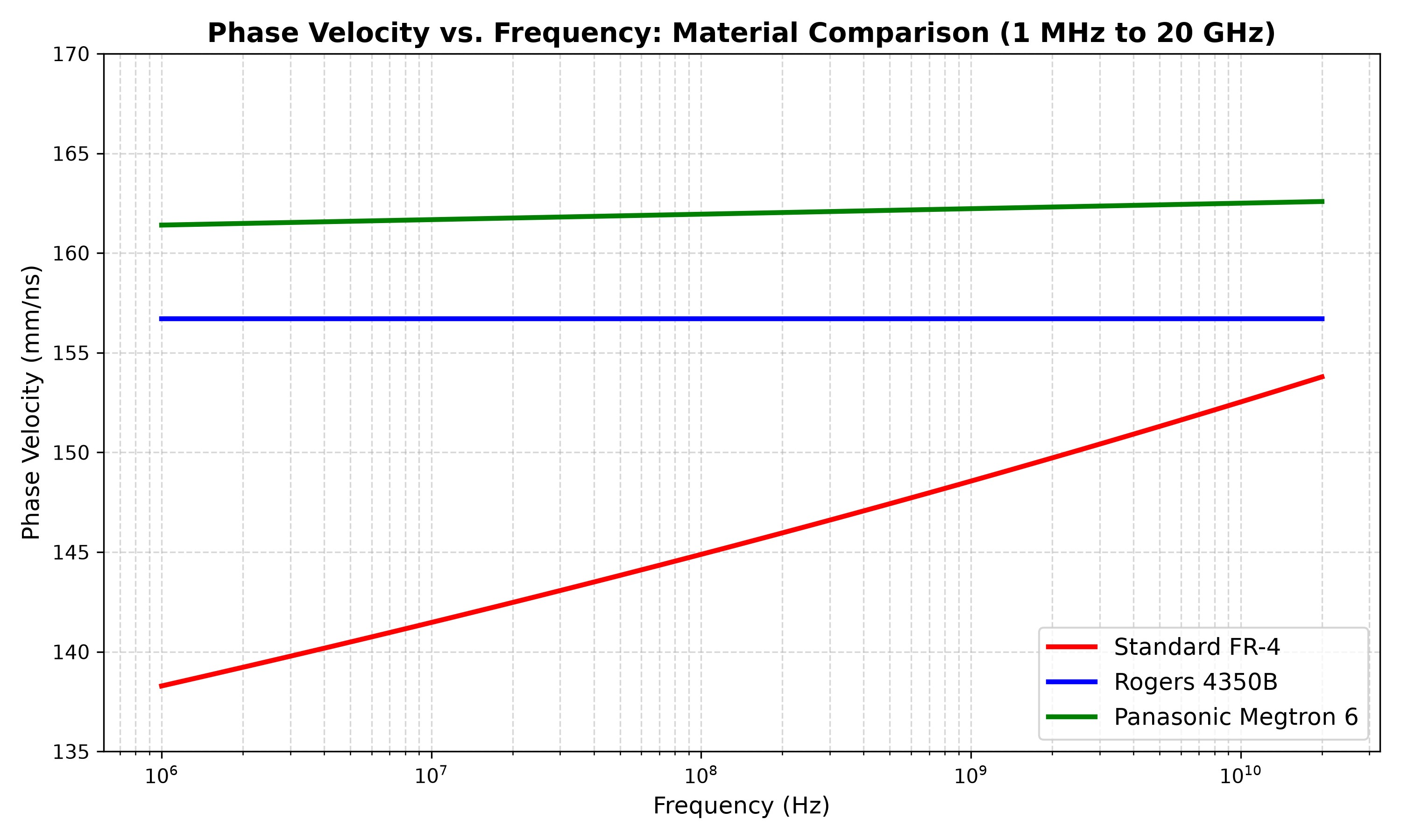
Figure 1. Phase velocity comparison of fr4 rogers and megtron 6.
Frequency-Dependent Dielectric Losses and Skew Amplification
As frequency rises, the dielectric loss tangent (Df) of FR-4 grows, attenuating high-frequency components more aggressively than low-frequency ones. This selective attenuation rounds off the fast edges that carry timing information, which shifts the receiver's threshold-crossing point in time. Two traces matched perfectly at DC can still exhibit meaningful skew at the signal's highest frequency component.
The Role of Signal Rise Time and Knee Frequency
The practical measure of how broadband a signal is the knee frequency. A square wave with a 1 ns rise time carries significant energy out to roughly 500 MHz, while one with a 100 ps rise time extends to about 5 GHz. The relationship is captured by the well-known approximation:
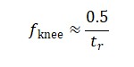
where tr is the 10-90% rise time. Above the knee frequency, the spectral energy of the edge falls off rapidly and contributes little to the signal's shape. Below it lies the energy that defines timing.
The knee frequency directly sets the required precision of length matching in a PCB. Consider a signal whose rise time yields a 5 GHz knee frequency. In FR-4, with a propagation velocity around 150 mm/ns, the wavelength at 5 GHz is roughly 30 mm.
The correct calculation for delay per millimeter is t=dv. Therefore, a 1 mm length mismatch at this frequency corresponds to approximately 6.67 ps of skew (t= 1mm/150mm/ns = 0.00667ns or 6.67 ps). This is a substantial slice of a 200 ps bit period at 5 Gbps, potentially closing a marginal eye.
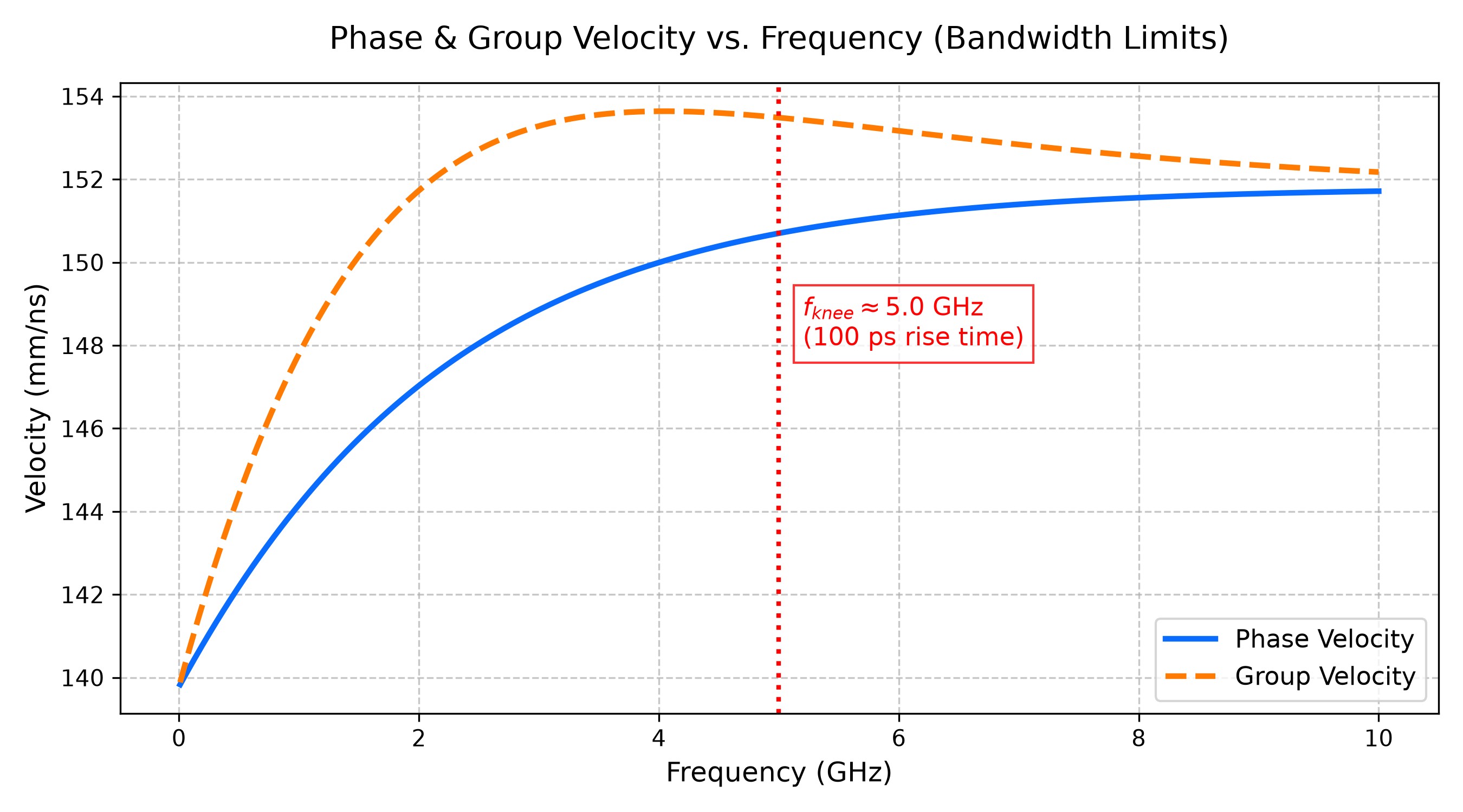
Figure 2. Phase and group velocity bandwidth limits on pcb stripline.
Differential Pair Length Matching Tolerance: How Much Skew Is Acceptable?
When establishing differential pair length matching guidelines, tolerance is not a fixed number. It is derived from how much timing error the system can absorb, set by three criteria:
- The bit period (unit interval). Faster data means less absolute time to spend on skew.
- The rise time and eye-diagram margin. A signal with generous eye height and width tolerates more skew than one already operating at the edge of its margin.
- The receiver's sensitivity. Some receivers include per-lane deskew and clock-data recovery; others do not, and demand tighter board-level matching.
Calculating the Skew Budget Based on Bit Period and Rise Time
A widely used engineering rule holds that intra-pair skew should stay within 5 to 10 percent of the UI. A complementary RF rule suggests keeping intra-pair skew below 1/20 to 1/10 of the wavelength corresponding to the fastest rise edge.
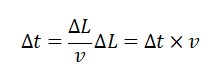
To move between the time domain and the physical domain, use the propagation velocity of the medium. It is critical to clearly distinguish between the velocity differences of outer-layer microstrips and inner-layer striplines. Outer layer microstrips propagate faster (often around 140-150 mm/ns) due to partial air exposure. Conversely, inner-layer striplines are slower (v ≈ 120− 140mm/ns for typical FR-4) because they are fully encased in the dielectric substrate.
From there, the conversions are simple:
Shifting From Length Matching to Time-Domain Delay Matching
The most important mindset shift in modern high-speed design is this: match on time-domain delay in picoseconds, not physical length in mils or millimeters. The reason is that physical length is only a reliable proxy for delay when the propagation velocity is constant everywhere along the path, and on a real multilayer board, it is not.
Note
A crucial clarification here separates the experts from the novices. While it is true that transitioning routing layers changes the effective dielectric constant and propagation velocity, via structures themselves introduce parasitic capacitance and inductance that alter the effective propagation velocity and add delay that pure length calculations ignore. Attributing signal slowdown exclusively to one or the other without acknowledging both the vias' parasitics and the layer transitions is a common and misleading oversimplification.
Comparative Guide: Serpentine vs. Sawtooth Length Matching
Once you know how much delay you need to add to a trace, you have to add it physically, and the shape of that added copper matters. The two predominant tuning techniques, serpentine and sawtooth, are optimized for different signaling situations. Choosing the wrong one can inject as much signal-integrity trouble as the skew it was meant to cure.
When to Implement Serpentine Length Matching
Serpentine length matching, routing a meandering, wavy pattern of parallel legs connected by bends, is best suited for single-ended signals or loosely coupled differential pairs where inter-trace coupling is minimal to begin with.
A widely cited guideline for serpentine routing is the 3W rule: keep the spacing between adjacent serpentine segments at least three times the trace width. The 3W rule is a rule of thumb, not a mandatory design rule.
- Signal-integrity sensitivity: faster edges and tighter budgets favor wider spacing.
- Routing density: congested boards may not afford full 3W spacing everywhere.
- Stackup: the distance to the reference plane influences how strongly adjacent legs couple.
Best Practices for Sawtooth Length Matching in Differential Pairs
Sawtooth tuning, adding short angled "teeth" to a trace, typically at a bend, is the preferred technique for tightly coupled differential pairs.
| Criterion | Serpentine | Sawtooth |
|---|---|---|
| Impedance discontinuity | Larger, long parallel detours perturb impedance | Minimal, only short local stubs are added |
| Coupling preservation | Poor for tight pairs, breaks coupling over the meander | Excellent, keeps the pair coupled through the adjustment |
| Tuning efficiency | Coarse, adds delay in larger increments | Fine-grained, small teeth give high-resolution control |
| Manufacturability | More sensitive to etch/geometry variation | Simpler geometry, more robust to process variation |
| Routing density | Consumes more board area | Compact, well suited to dense, high-speed regions |
Reference Table: High-Speed Interface Length Matching Recommendations
Calculation Note: The physical length equivalent is derived using ∆L = ∆t×v, assuming a standard outer-layer signal velocity of v ≈ 150mm/ns (which equates to roughly 5.9 mils/ps).
| Protocol | Typical Data Rate | Intra-Pair Delay Target (ps) | Inter-Pair Delay Target (ps) | Physical Length Equivalent (mils/mm)* | Preferred Tuning Method |
|---|---|---|---|---|---|
| USB4 / USB Type-C | 40 Gbps (USB4 Gen 3, 20 Gbps/lane) | 10 ps intra-pair | 75 ps (lane-to-lane, application-dependent) | 59 mils/1.50 mm | Sawtooth |
| HDMI 2.1 | 48 Gbps (12 Gbps/lane FRL) | 1-5 ps intra-pair | 10 ps (channel-to-channel) | 5.9−29.5 mils/0.15−0.75 mm | Sawtooth |
| DDR5 | Up to 6400 MT/s | 1-2 ps (DQ/DQS within byte) | 30-50 ps (address/command group) | 5.9−11.8 mils/0.15−0.30 mm | Serpentine (DQ byte lanes), sawtooth at bends |
| PCIe Gen 5 | 32 GT/s | 5 ps intra-pair | 30 ps (lane-to-lane, vendor-dependent) | 29.5 mils/0.75 mm | Sawtooth |
| PCIe Gen 6 | 64 GT/s (PAM4) | 0.5-1 ps intra-pair | 15 ps (lane-to-lane, vendor-dependent) | 2.95−5.9 mils/0.075−0.15 mm | Sawtooth |
FAQ about PCB Trace Length Matching vs Frequency
Does clock frequency determine PCB trace length matching requirements?
No. Clock frequency is misleading on its own because digital signals are broadband. What sets the effective bandwidth, and therefore the matching requirement, is the signal's rise time, not its fundamental frequency. A slow 10 MHz clock with a sharp 100 ps edge contains frequency content comparable to a 5 GHz signal and demands equally strict length matching.
What is the difference between serpentine and sawtooth length matching?
Serpentine tuning uses a meandering, wavy pattern of parallel legs to add length, and is best for single-ended signals or loosely coupled pairs. Sawtooth tuning adds short angled teeth to a trace, preserving coupling and minimizing impedance discontinuity, which makes it the preferred choice for tightly coupled differential pairs, especially at bends.
Why does my length-matched differential pair still show skew?
Because physical length is only a proxy for delay. Skew can persist when the two traces traverse different layers with different dielectric constants, pass through different via counts, encounter fiber-weave Dk variation, or experience frequency-dependent loss differently. The fix is to match on time-domain delay in picoseconds rather than on physical length.
How tight should intra-pair skew be for high-speed interfaces?
A common rule of thumb keeps intra-pair skew within 5 to 10 percent of the unit interval (bit period). An alternative RF-oriented rule keeps it below 1/20 to 1/10 of the wavelength at the signal's fastest rise edge. The exact figure depends on the protocol and should be confirmed against the device vendor's layout guidelines; serial links such as PCIe Gen 5 and USB4 demand single-digit-picosecond intra-pair matching, with next-generation interfaces like PCIe Gen 6 pushing toward sub-picosecond targets.
Conclusion: Demystifying PCB Trace Length Matching vs Frequency
Rise time rules, not clock speed. The instinct that a higher clock rate automatically demands tighter matching confuses the carrier with the signal's true bandwidth, and the corollary instinct that equal physical length guarantees equal arrival ignores dielectric dispersion, layer transitions, and frequency-dependent loss.
Keep Learning
Demystifying PCB Trace Length Matching vs Frequency: Ultimate Guide
Key Takeaways Signal rise time, not clock frequency, is the true determinant of trace length matching tolerance. A 10 MHz clock with a 100 ps rise time behaves like a GHz signal and demands strict matching. Dielectric dispersion causes phase velocity to shift across the spectrum, invalidating single-frequency matching assumptions. Designers should match by time-domain delay in picoseconds, not by physical length in mils. Serpentine routing suits single-ended traces, while sawtooth tuning preserves cou......
Bias Tee Design and PCB Layout: Guide for RF Engineers
Key Takeaways A bias tee lets DC power and an RF signal share one trace, using just an inductor and a capacitor. No separate DC line needed. Pick L and C using two simple rules: the inductor's reactance should be at least 10x the system impedance, and the capacitor's reactance should be at most one tenth of it. Layout matters as much as the math. A few extra millimeters of trace at the L-C junction can shift the whole frequency response. Three habits keep a bias tee working as designed: controlled imp......
PCB Routing Rules: Essential Guidelines & Best Practices
Key Takeaways 1. Placement Drives Routing: Good component placement, grouped by functional block with decoupling caps adjacent to IC power pins, determines 70% of routing success before the first trace is drawn. 2. Master Trace Width & Spacing: Size traces per IPC-2152 for current-carrying capacity and maintain center-to-center spacing of at least 3W between adjacent traces to suppress crosstalk. 3. Build a Solid Layer Stackup: Every signal layer must sit adjacent to a continuous reference plane to de......
PCB Teardrop You Should Know
In the design and manufacturing of PCBs (Printed Circuit Boards), the teardrop (Pad Tear Drop) plays a vital role. It is not only the connection point between electronic components and PCB, but it can also enhance the soldering strength and improve stability. This article will delve into what a PCB teardrop is, what it does, and how to set up a PCB teardrop to help you better understand and apply this key technology. What is a PCB Teardrop? PCB teardrops are small drops of solder material that form ar......
Mastering PCB Routing Techniques for Optimal Circuit Design and Performance
Introduction PCB routing is a fundamental and intricate aspect of circuit design that significantly influences the performance, reliability, and functionality of electronic devices. Effective PCB routing techniques are critical for optimizing electrical traces, maintaining signal integrity, and ensuring the overall efficiency of the PCB layout. This comprehensive guide will explore various PCB routing techniques, from trace optimization and signal path management to high-speed PCB routing and layout d......