Bias Tee Design and PCB Layout: Guide for RF Engineers
13 min
- Introduction
- What Is a Bias Tee? Understanding the Basics
- Bias Tee Design Principles for RF Engineers
- PCB Layout Best Practices for Bias Tee Circuits
- Common Bias Tee PCB Layout Mistakes and How to Avoid Them
- Simulating Your Bias Tee Design Before PCB Fabrication
- FAQ about Bias Tee Design
Key Takeaways
A bias tee lets DC power and an RF signal share one trace, using just an inductor and a capacitor. No separate DC line needed.
Pick L and C using two simple rules: the inductor's reactance should be at least 10x the system impedance, and the capacitor's reactance should be at most one tenth of it.
Layout matters as much as the math. A few extra millimeters of trace at the L-C junction can shift the whole frequency response.
Three habits keep a bias tee working as designed: controlled impedance routing, tight component placement, and a solid ground plane.
Simulate the design in SPICE before you lay it out. It catches problems while they are still cheap to fix.
Introduction
Every RF engineer runs into this problem at some point. A power amplifier or an antenna needs steady DC power. But the same trace is carrying an RF signal, and that signal cannot handle a bulky choke or an extra connector in the way.
This is where a bias tee comes in. It is a simple circuit that lets DC and RF share one conductor. No separate DC line needed. Just two parts do the job: an inductor and a capacitor.
But knowing the theory is not enough. The same bias tee can behave very differently on a real board, depending on trace length, component footprint, and how you handle the ground plane. This guide covers the basics, the design math, and the PCB layout choices that decide whether your bias tee works as intended or turns into a debugging headache.
What Is a Bias Tee? Understanding the Basics
A bias tee has three ports: a DC port, an RF port, and a combined output where RF and DC meet. An inductor connects the DC supply to that output. A capacitor connects the RF source to the same output. On a PCB, you can build this from two discrete parts, or at lower frequencies, from copper geometry alone.
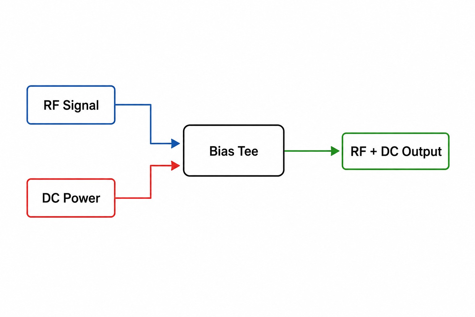
Figure 1: Basic bias tee circuit diagram
Bias Tee Symbol and Circuit Diagram Explained
A typical bias tee circuit diagram shows three ports meeting at one node. The DC path runs through an inductor (L). The RF path runs through a capacitor (C). Both meet at the same point, and the combined signal leaves from there toward the load, whether that's an amplifier, an antenna, or a photodiode.
The bias tee symbol you'll see in RF block diagrams is usually a T-shaped junction, with L on the DC leg and C on the RF leg.
Here's the simple version of how it works. The inductor blocks RF but passes DC. The capacitor passes RF but blocks DC. That's the whole idea behind a bias tee. No magic, just two components doing opposite jobs at the same frequency.
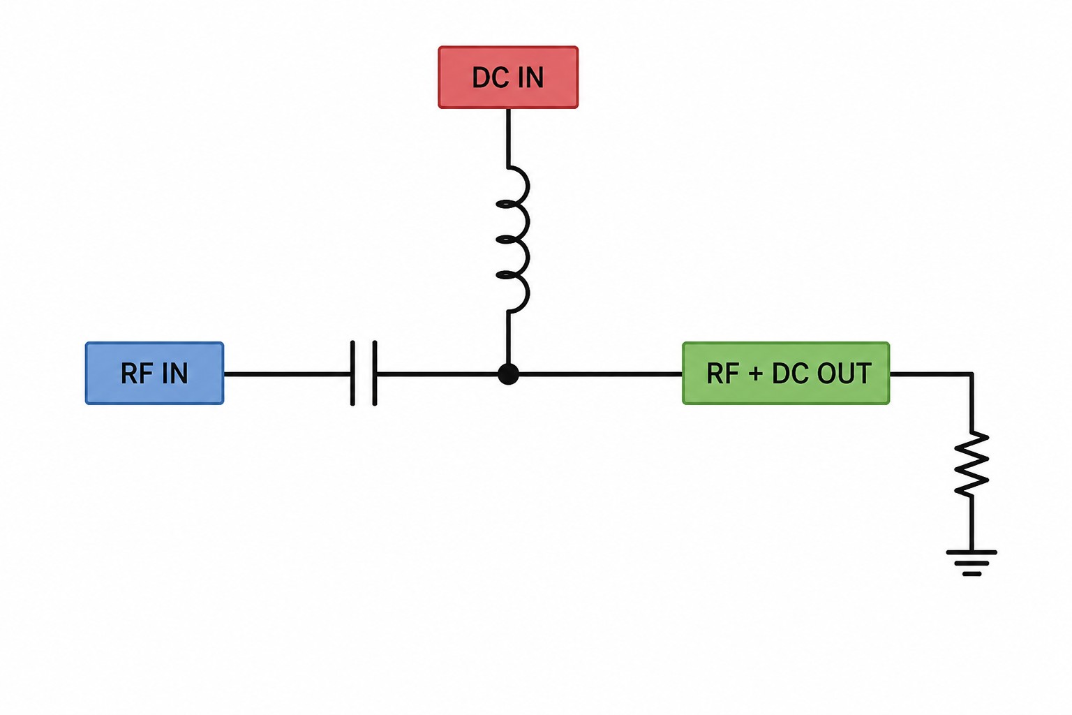
Figure 2: Bias tee schematic showing RF input through a capacitor and DC input through an inductor combining into a shared RF + DC output
What Is a Bias Tee Used For? Key Applications in RF Systems
So what is a bias tee used for? The most common job is powering RF amplifiers, especially low-noise and power amplifiers that need DC right at their RF pin.
Photodiode biasing is another common use. The bias tee supplies reverse-bias voltage to the photodiode while letting the signal pass through cleanly.
You'll also find bias tees in antenna feed networks, where one cable carries both the RF signal and DC power for an active part like a tower-mounted amplifier. Laser drivers use the same trick, combining a modulation signal with DC bias current.
In every case, the reason is the same. DC and RF need to share one conductor, and an rf bias tee is the simplest way to make that happen without extra traces or connectors. Fewer parts also means fewer places for something to go wrong on the board.
Bias Tee Design Principles for RF Engineers
Picking L and C values is only half the job. Those values set the theoretical passband, but layout decides how close you get to that theory in real life. Tools like EasyEDA can help with the LC math, but it's worth understanding where the numbers come from.
Impedance Ratio and Component Value Selection
Bias tee design comes down to two simple rules, both based on the system impedance Z0 (usually 50 ohms).
Here's what those rules give you at a few common frequency bands:
| Frequency Band | Min. Inductance (L) | Practical L Value | Min. Capacitance (C) | Practical C Value |
|---|---|---|---|---|
| 900 MHz | ≥ 88.4 nH | 100 nH | ≥ 35.4 pF | 39 pF |
| 2.4 GHz | ≥ 33.2 nH | 39 nH | ≥ 13.3 pF | 15 pF |
| 5.8 GHz | ≥ 13.7 nH | 15 nH | ≥ 5.5 pF | 6.8 pF |
A higher reactance ratio improves low-frequency isolation but pushes the low-end cutoff higher, which effectively narrows the usable bandwidth. Check the design against your actual operating bandwidth, not just one center frequency. Once you have L and C, EasyEDA can help you calculate the matching trace geometry.
LC Bias Tee Frequency Response and Filter Design
An LC bias tee is not flat across every frequency. It has a passband where the reactance rules above hold true. Outside that band, power delivery drops and the impedance mismatch grows.
If you need a wider passband or better noise rejection, you can add extra filtering on the DC line, like a shunt capacitor or a ferrite bead. This adds complexity, so weigh it against the board space it costs.
Design Tip
Before you lay anything out, run a quick SPICE simulation across your target frequency range. It's much easier to spot a mismatch on a plot than after the board comes back from fab.
PCB Layout Best Practices for Bias Tee Circuits
A bias tee is only as good as its layout. Even perfect L and C values can be ruined by a bad board design. Three things matter most: controlled impedance on the RF path, tight component placement, and a solid ground plane. Get those three right and the rest tends to fall into place.
Controlled Impedance Routing for RF Bias Tee Traces
The RF path from the capacitor to the output needs to be a controlled impedance line, usually a 50 ohm microstrip or coplanar waveguide.
Trace width depends on your stackup, mainly the dielectric thickness and distance to the nearest ground plane. Most PCB tools have a built-in impedance calculator for this — JLCPCB's impedance calculator, for example, lets you enter your board thickness, copper weight, and dielectric constant to get the right trace width for a 50 ohm line.
Any impedance discontinuity along this trace, whether from a width change, a via, or a sharp bend, causes reflections and power loss. Keep the RF trace short and straight. The DC trace matters less for impedance, but keep it wide enough to avoid resistive losses.
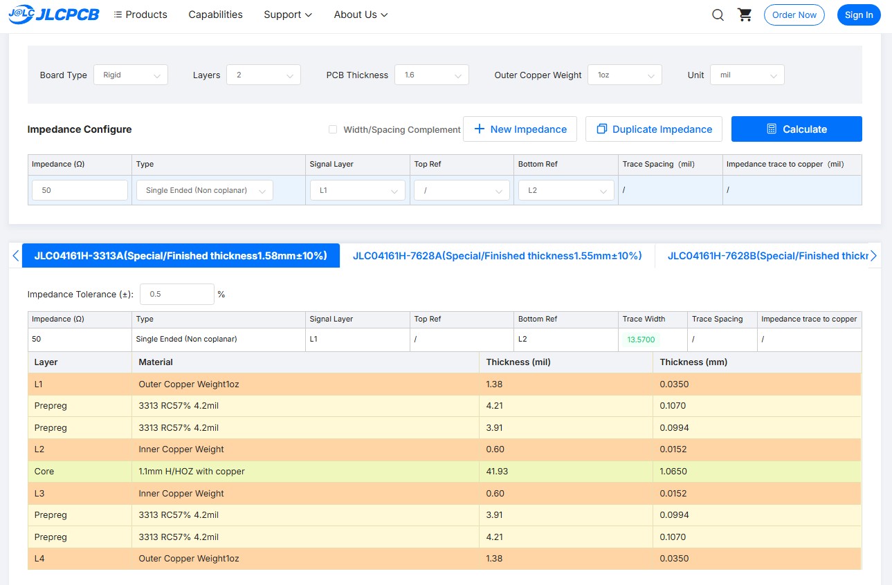
Figure 3: JLCPCB impedance calculator showing 50 ohm single-ended trace width calculation with PCB stackup layers
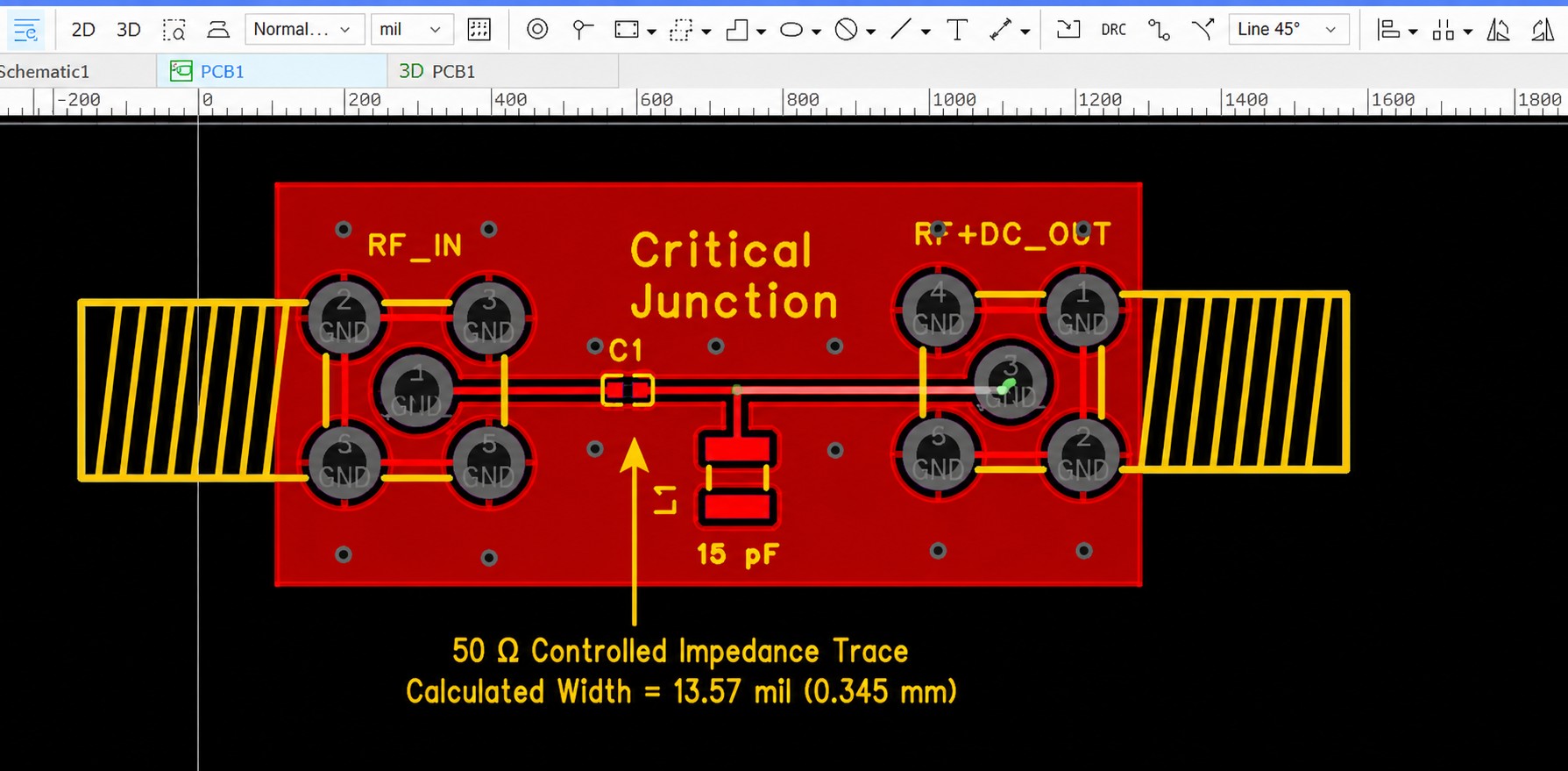
Figure 4: EasyEDA PCB layout showing the critical L-C junction with 15 pF capacitor on a 50 ohm controlled impedance trace
Component Placement and Parasitic Minimization on PCB
Placement matters more here than in most passive circuits. Keep the inductor and capacitor as close together as you physically can. The junction between L, C, and the output trace is the most sensitive point on the board.
Every extra millimeter of trace at this junction adds parasitic inductance, and that shifts your frequency response away from the design.
Package size matters too. 0402 or 0603 parts work best for GHz-range bias tees, since smaller packages mean less parasitic inductance. Larger packages like 1206 can cause self-resonance issues well below your target frequency.
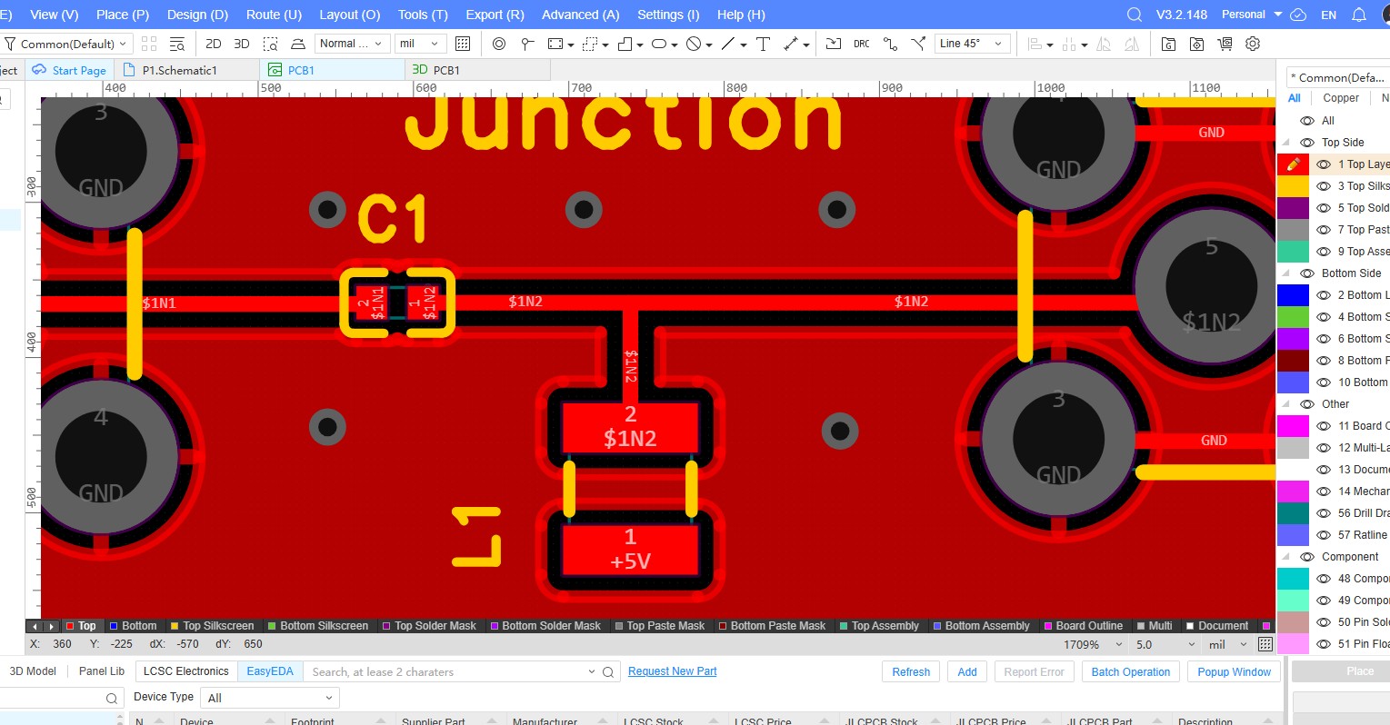
Figure 5: EasyEDA bias tee component placement showing tight L-C junction spacing
Ground Plane, Via Stitching, and RF Isolation Techniques
A solid, unbroken ground plane under the bias tee is essential. It gives you the low-inductance return path that RF performance depends on.
Where you can, add via stitching along both sides of the RF trace. This forms a coplanar waveguide with ground and adds extra isolation. Avoid any ground plane splits under the bias tee region. A split here acts just like a trace impedance mismatch and reflects power.
On multi-layer boards, put the bias tee on the top layer with the ground plane on layer 2, as close to the top as possible. This keeps the loop area small. Most PCB tools let you set DRC rules that flag ground plane gaps automatically, which is a good safety net.
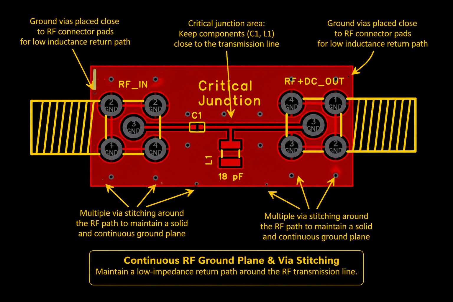
Figure 6: EasyEDA ground plane and via stitching for bias tee RF isolation
Ready to layout your bias tee or RF circuit? Submit your schematic to get professional feedback and precision routing before manufacturing—plus, claim a $105 coupon to get expert layout service for almost free!
Get Free Trial
Common Bias Tee PCB Layout Mistakes and How to Avoid Them
Most bias tee failures are not about bad math. They come from layout mistakes that are easy to miss on a schematic review. These mostly fall into two buckets: parasitic effects and routing errors. Both are easy to fix once you know where to look.
Parasitic Inductance and Capacitance from Poor Layout
Long or thin traces add parasitic inductance. Component pads placed too close to a ground plane, or traces coupling to nearby copper, add parasitic capacitance. Both push your bias tee's frequency response off target.
Quick Formula
A 5 mm trace between the inductor and capacitor adds about 3 nH of parasitic inductance. At 2.4 GHz, that's roughly 45 ohms of reactance — more than enough to change how the whole circuit behaves.
The fix is simple. Keep the L-C junction trace as short as possible. Use wide traces on the DC path to cut series inductance. Add ground stitching vias around the RF path.
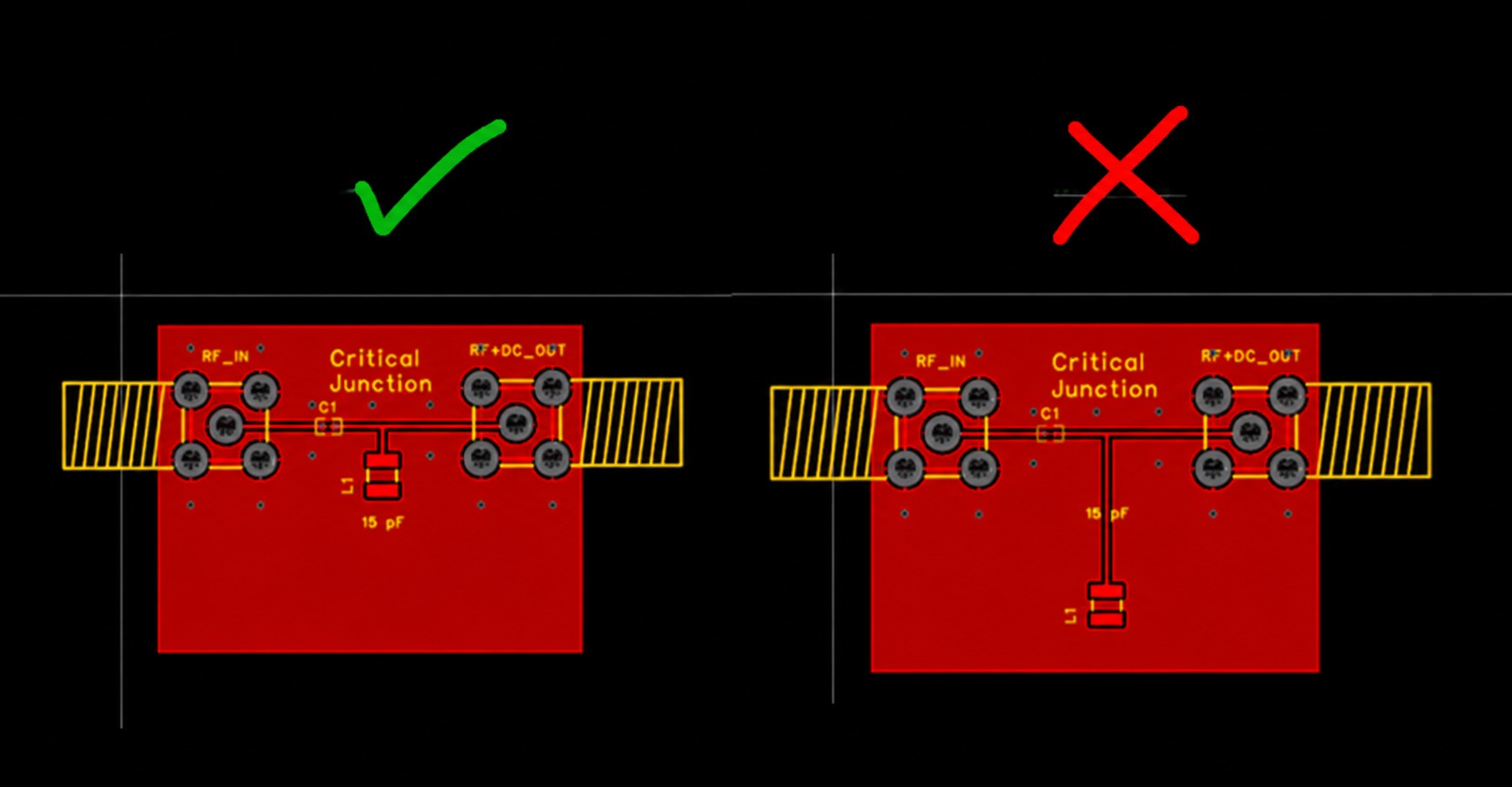
Figure 7: Comparison of correct versus incorrect capacitor placement at the bias tee L-C junction, showing trace length impact on parasitic inductance
Trace Routing and Ground Plane Errors That Degrade Performance
Three routing mistakes show up again and again.
Common Routing Mistakes to Avoid
- Routing the RF output trace over a gap in the ground plane. This creates a discontinuity and reflects power back toward the source.
- Using the wrong trace width for your target impedance. On 1.6 mm standard FR4 with a single ground plane on the bottom layer, a 50 ohm line needs to be about 2.9 mm wide. With a thin dielectric between the top layer and an inner ground plane, like a 0.2 mm prepreg, that same 50 ohm trace can narrow to around 0.35 mm.
- Routing high-speed digital signals parallel to the RF path without enough spacing. This lets digital noise couple straight into your RF signal.
The fixes are straightforward: keep a continuous ground reference under the RF trace, use the correct trace width for your stackup, and leave at least three times the trace width as spacing between RF and digital traces.
Simulating Your Bias Tee Design Before PCB Fabrication
Simulation is the step that connects theory to a working PCB. It's worth doing before you route a single trace.
-
AC Analysis
Run an AC analysis to show the frequency response and confirm the passband sits where you expect.
-
Transient Analysis
A transient analysis shows power-up behavior, including any voltage overshoot as the capacitor charges.
-
Impedance Sweep
An impedance sweep at the output shows how close you are tracking 50 ohms across your band.
Use realistic parasitic models, not ideal components. Add ESR and ESL for the capacitor, and equivalent parallel capacitance (EPC) for the inductor. If the simulation shows the design is sensitive to just a few nH of added inductance, that's your signal to keep the PCB layout extra tight around the L-C junction.
FAQ about Bias Tee Design
Q: Can a bias tee be built entirely from PCB copper, without discrete parts?
At lower frequencies, yes. A spiral trace can act as the inductor, and a gap in the copper can act as the capacitor. For most GHz-range rf bias tee designs, discrete SMD parts give you tighter control.
Q: What happens if the inductor value is too low?
The inductor starts loading the RF path. RF energy leaks toward the DC supply, and less power reaches your intended load.
Q: Does a bias tee clean up noise on the DC supply?
No. A basic bias tee only separates DC and RF. It does not filter noise. If your supply is noisy, add filtering on the DC line as well.
Q: How much isolation should a bias tee provide?
It depends on the application, but 20 to 30 dB at your operating frequency is a reasonable target for most amplifier and antenna feed designs.
Q: Do I need a bias tee for every RF design?
No. If your DC and RF paths can be routed separately without space or interference issues, a bias tee is not required. It's most useful when board space is tight or a single trace has to carry both.
Conclusion about Bias Tee Design
A bias tee looks simple on paper, just an inductor and a capacitor. But its real-world performance depends as much on PCB layout as on component choice.
Controlled impedance routing, minimal parasitics at the L-C junction, and a solid ground plane are what save you from costly debugging and re-spins. The design math is easy once you know the reactance rules. The hard part is turning that math into good copper. Take the layout as seriously as the schematic, and your bias tee will work the first time.
If you're working on a bias tee or another RF circuit, JLCPCB's layout services can handle your complete placement and routing and review your design and impedance control before fabrication while it's still easy to fix.
Keep Learning
Demystifying PCB Trace Length Matching vs Frequency: Ultimate Guide
Key Takeaways Signal rise time, not clock frequency, is the true determinant of trace length matching tolerance. A 10 MHz clock with a 100 ps rise time behaves like a GHz signal and demands strict matching. Dielectric dispersion causes phase velocity to shift across the spectrum, invalidating single-frequency matching assumptions. Designers should match by time-domain delay in picoseconds, not by physical length in mils. Serpentine routing suits single-ended traces, while sawtooth tuning preserves cou......
Bias Tee Design and PCB Layout: Guide for RF Engineers
Key Takeaways A bias tee lets DC power and an RF signal share one trace, using just an inductor and a capacitor. No separate DC line needed. Pick L and C using two simple rules: the inductor's reactance should be at least 10x the system impedance, and the capacitor's reactance should be at most one tenth of it. Layout matters as much as the math. A few extra millimeters of trace at the L-C junction can shift the whole frequency response. Three habits keep a bias tee working as designed: controlled imp......
PCB Routing Rules: Essential Guidelines & Best Practices
Key Takeaways 1. Placement Drives Routing: Good component placement, grouped by functional block with decoupling caps adjacent to IC power pins, determines 70% of routing success before the first trace is drawn. 2. Master Trace Width & Spacing: Size traces per IPC-2152 for current-carrying capacity and maintain center-to-center spacing of at least 3W between adjacent traces to suppress crosstalk. 3. Build a Solid Layer Stackup: Every signal layer must sit adjacent to a continuous reference plane to de......
PCB Teardrop You Should Know
In the design and manufacturing of PCBs (Printed Circuit Boards), the teardrop (Pad Tear Drop) plays a vital role. It is not only the connection point between electronic components and PCB, but it can also enhance the soldering strength and improve stability. This article will delve into what a PCB teardrop is, what it does, and how to set up a PCB teardrop to help you better understand and apply this key technology. What is a PCB Teardrop? PCB teardrops are small drops of solder material that form ar......
Mastering PCB Routing Techniques for Optimal Circuit Design and Performance
Introduction PCB routing is a fundamental and intricate aspect of circuit design that significantly influences the performance, reliability, and functionality of electronic devices. Effective PCB routing techniques are critical for optimizing electrical traces, maintaining signal integrity, and ensuring the overall efficiency of the PCB layout. This comprehensive guide will explore various PCB routing techniques, from trace optimization and signal path management to high-speed PCB routing and layout d......