Comparison of BGA vs LGA in High-Power Applications
9 min
- Understanding BGA and LGA Packages:
- Thermal Considerations for BGA Packages:
- Thermal Considerations for LGA Packages:
- Industry Applications and Case Studies:
- Case Studies:
- FAQ about Comparison of BGA vs LGA
- Conclusion:
Key Takeaways
In high-power PCB designs, BGA and LGA packages offer strong high I/O performance but require effective thermal management. BGA excels with solder balls and thermal vias, while LGA relies on direct pad contact with TIMs and thermal pads. Key to success are thermal vias, thicker copper layers, ground planes, and simulations to reduce thermal resistance and maintain reliable junction temperatures.
As electronic devices continue to shrink in size while increasing in performance, managing heat dissipation has become a critical consideration in PCB design. Two popular package styles used in high-power applications are ball grid array (BGA) and land grid array (LGA). While both BGA and LGA offer unique advantages, they possess distinct structural features that result in different thermal characteristics. This article will provide an overview of BGA and LGA packages, explore the thermal challenges at high power levels, and discuss design considerations and solutions for effective thermal management.
Understanding BGA and LGA Packages:
A ball grid array (BGA) package utilizes a grid of solder balls underneath the IC chip to connect with the PCB. The balls provide an electrical connection, while also facilitating heat transfer from the die to the board through the solder balls. BGAs are widely used for their high I/O density, electrical performance, and ability to scale to large die sizes.
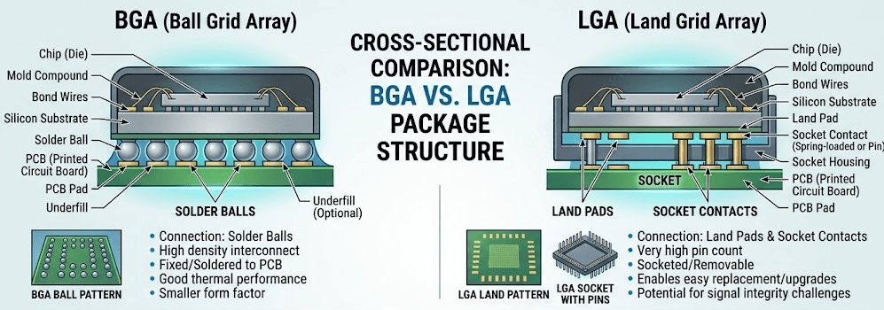
In contrast, a land grid array (LGA) utilizes metal pads rather than solder balls to make contact with the PCB. An LGA requires an interposer or retention mechanism to ensure adequate contact pressure between the IC pads and PCB lands. While LGAs do not solder to the board, they facilitate heat transfer through the pad contacts. LGAs offer advantages such as reworkability and reduced stresses compared to BGAs.
For high-power applications, both packages support complex ICs with high I/O counts. However, the heat fluxes generated—often exceeding 100-500 W in demanding scenarios—require optimized PCB layouts to prevent thermal throttling and ensure long-term reliability.
Thermal Considerations for BGA Packages:
For BGA packages, the solder balls provide the main conduit for heat transfer from the die to the PCB. To maximize the BGA’s thermal performance, the PCB must be designed to effectively spread heat laterally and transfer it to the board edge or to a heat sink.
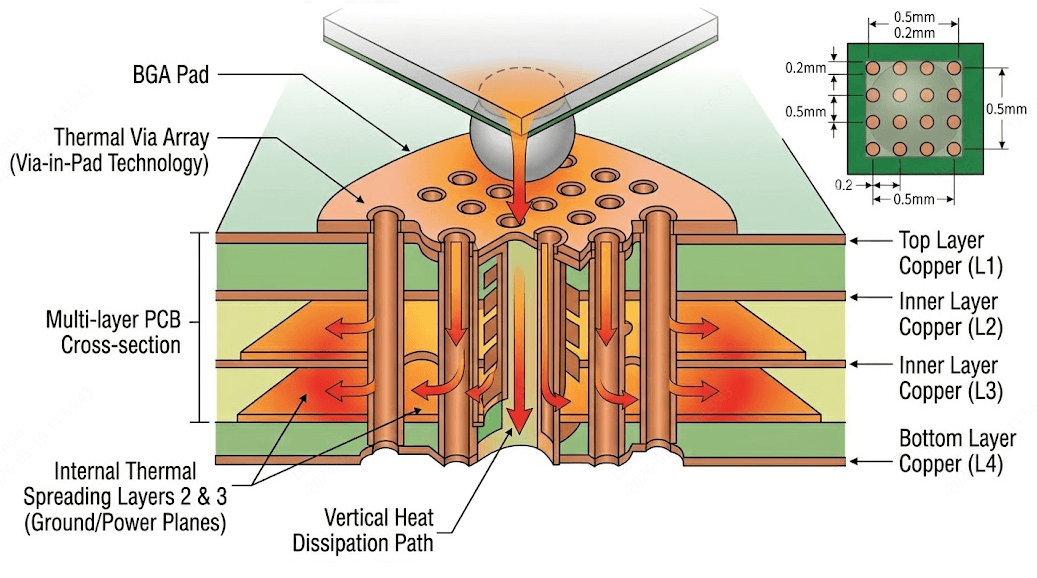
One technique is to place thermal vias underneath the BGA pads on the PCB. The thermal vias provide a direct thermal conduction path to inner board layers or bottom ground planes. This minimizes the heat spreading distance to extract heat from the package. High thermally conductive materials, such as copper paste or conductive epoxy, should be used to fill vias where possible, as air-filled or standard plated vias have significantly higher thermal resistance.
Increasing the number of thermal vias reduces the package’s junction-to-board thermal resistance. For example, a dense array of 0.3 mm diameter vias on a 1 mm pitch can reduce thermal resistance by 40-70% depending on board stackup and copper thickness, though exact gains require simulation. However, too many vias can compromise solder joint reliability due to reduced solder volume and potential CTE mismatch stresses. Tradeoffs must be evaluated to optimize heat transfer while minimizing mechanical stresses on solder balls. Designers often use via-in-pad techniques for fine-pitch BGAs (0.5 mm or below) to maintain routing density without sacrificing thermal paths.
Larger copper pads on the PCB will also improve heat spreading from BGA solder balls.Thicker copper layers (1 oz or 2 oz) enhance in-plane thermal conductivity.Thermal simulations help predict temperature gradients and identify hot spots underneath BGAs. Copper heat sinks or thermal slugs embedded in the PCB can further augment heat dissipation. In practice, combining thermal vias with dedicated ground planes and external heatsinks or liquid cooling interfaces is common in high-power designs exceeding 100 W.
Thermal Considerations for LGA Packages:
LGAs rely on conduction through the interface between the package pads and PCB lands to transfer heat. As such, the thermal interface is critical for minimizing thermal resistance. LGAs intended for high-power use will incorporate thermal pads rather than electrical pads on some array locations to maximize heat transfer.
The application of thermal interface materials (TIMs) between LGA pads and lands is essential to fill surface voids and improve heat conduction. Typically, a thermally conductive paste or film TIM is applied to the LGA or PCB lands before assembly. The TIM should exhibit high thermal conductivity (e.g., 5-15 W/m·K or higher) and be sufficiently compliant to accommodate surface roughness, flatness tolerances, and minor warpage under pressure.
Thermal vias in the PCB underneath LGA thermal pads further enhance heat extraction. Similar to BGA designs, dense via arrays connected to thick copper planes provide vertical heat paths, while larger thermal pad areas improve contact efficiency. As with BGAs, thermal simulations of the LGA and PCB assembly are important when evaluating thermal performance. Factors such as LGA land dimensions, via quantity, TIM thickness, and contact pressure must be modeled to achieve the required heat dissipation. Proper clamping force from the retention mechanism is also vital to maintain consistent low thermal resistance over time and temperature cycles.
Table: Key Thermal Design Comparison Between BGA and LGA
| Aspect | BGA | LGA | Common Best Practice |
|---|---|---|---|
| Primary Heat Path | Solder balls + thermal vias | Direct pad contact + TIM | Dense thermal vias + copper planes |
| Thermal Resistance Impact | Good with via arrays (40-70% reduction possible) | Excellent with optimized TIM & pressure | Thermal simulation mandatory |
| Rework / Reliability | Solder joints more stress-prone | Higher reworkability, lower stress | Evaluate CTE and via density |
| High Power Suitability | Strong for soldered high I/O | Strong for large thermal pads | Combine with 1-2 oz copper & heatsinks |
Industry Applications and Case Studies:
BGA and LGA packages find extensive applications across various industries, including telecommunications, automotive, aerospace, and consumer electronics. Let's explore some notable industry applications and case studies:
Telecommunications:
BGA and LGA packages are widely used in high-performance networking equipment, such as routers, switches, and base stations. These applications demand efficient thermal management due to the high-power components involved. By implementing optimized thermal design strategies, manufacturers have achieved reliable operation and extended product lifespans.
Automotive:
In the automotive industry, BGA and LGA packages are employed in electronic control units (ECUs), sensors, and infotainment systems. The stringent temperature requirements and harsh operating conditions in vehicles necessitate robust thermal management solutions. Through careful PCB design and thermal simulations, automotive electronics have been able to maintain optimal performance under extreme temperature environments.
Aerospace:
BGA and LGA packages are utilized in avionics systems, satellite communication equipment, and flight control systems. Aerospace applications demand exceptional reliability and thermal performance due to the critical nature of these systems. By incorporating advanced cooling techniques, such as heat pipes and liquid cooling, engineers have successfully managed heat dissipation and ensured thesafe operation of aerospace electronics.
Consumer Electronics:
BGA and LGA packages are prevalent in consumer electronic devices, including smartphones, tablets, gaming consoles, and high-end audio equipment. These devices often require compact form factors while delivering high computing power, making thermal management crucial. Through innovative thermal solutions such as vapor chambers, heat spreaders, and advanced cooling techniques, manufacturers have enhanced device performance and prevented overheating issues.
Case Studies:
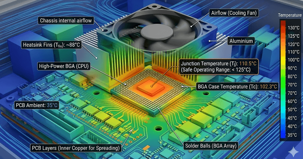
In 5G base station radios, BGAs efficiently dissipate heat from high-power mmWave beamforming ICs. Thermal vias, copper pads, and heat sinks maintain junction temperatures safely below 125°C despite 200W+ heat fluxes, enabling continuous high-throughput operation.
LGA processors in high-performance computing clusters use large thermal pads to conduct heat to liquid cold plates. The direct contact cooling maintains 45°C chip temperatures under 500W.
In radar and electronic warfare systems, stacked BGA memory devices with thermal vias handle 300W per module. The vias connect to thick center ground layers in multilayer boards to spread heat.
FAQ about Comparison of BGA vs LGA
Q: What is the main difference between BGA and LGA packages?
BGA packages use an array of solder balls for electrical and thermal connection to the PCB, while LGA packages use flat metal pads that require a retention mechanism for contact pressure. BGA offers easier soldering but higher mechanical stress, whereas LGA provides better reworkability and lower stress on the board.
Q: Which package is better for high-power applications — BGA or LGA?
Both are suitable for high-power use, but the choice depends on specific needs. BGA excels in high I/O density and soldering reliability, while LGA is often preferred when large dedicated thermal pads and easier rework are required. Effective thermal management (vias, TIMs, copper planes) is more critical than the package type itself.
Q: How do thermal vias improve heat dissipation in BGA packages?
Thermal vias placed underneath BGA pads create direct vertical heat conduction paths from the solder balls to inner copper layers or ground planes. A dense array of vias can significantly reduce junction-to-board thermal resistance (θjb), often by 40-70%, helping maintain safe operating temperatures in high-power designs.
Q: Why are Thermal Interface Materials (TIMs) important for LGA packages?
TIMs fill microscopic air gaps between LGA pads and PCB lands, dramatically reducing thermal resistance at the critical interface. Using high-conductivity TIMs (5–15 W/m·K or higher) combined with proper contact pressure ensures efficient heat transfer, especially when paired with thermal pads and vias.
Q: Should I use thermal simulations when designing with BGA or LGA packages?
Yes. Thermal simulations are highly recommended to predict temperature gradients, identify hotspots, and optimize via placement, copper thickness, and stackup before manufacturing. They help balance thermal performance with mechanical reliability and prevent costly design iterations.
Q: What PCB design techniques best support high-power BGA and LGA applications?
Key techniques include using dense thermal vias (possibly via-in-pad), thicker copper layers (1oz or 2oz), dedicated ground/power planes for heat spreading, larger thermal pads, and Metal Core PCBs for extreme heat dissipation. Proper via filling and strategic heatsink integration further enhance performance.
Conclusion:
In conclusion, both BGA and LGA packages offer unique advantages and challenges in terms of thermal characteristics. By understanding the specific thermal considerations for each package style and implementing appropriate design solutions, you can effectively manage heat dissipation and enhance the performance and longevity of high-power electronic systems.
When it comes to manufacturing electronic systems, JLCPCB is your reputable and reliable provider of PCB fabrication and assembly services. Click the botton below to empower your next electronic project!
Keep Learning
Comparison of BGA vs LGA in High-Power Applications
Key Takeaways In high-power PCB designs, BGA and LGA packages offer strong high I/O performance but require effective thermal management. BGA excels with solder balls and thermal vias, while LGA relies on direct pad contact with TIMs and thermal pads. Key to success are thermal vias, thicker copper layers, ground planes, and simulations to reduce thermal resistance and maintain reliable junction temperatures. As electronic devices continue to shrink in size while increasing in performance, managing he......
A Complete Guide to IC Package: Types, Properties, PCB Design Rules & Selection Tips
What is an IC Package? An IC package is the physical enclosure that houses an integrated circuit or electronic component, providing mechanical protection, electrical connections, and thermal management. It ensures that the component can be reliably mounted on a PCB and integrated into circuits. Key Functions of an IC Package: 1. Mechanical protection: Shields the chip from physical damage and environmental factors. 2. Electrical connections: Provides pins or solder balls to connect the IC to the PCB. ......
BGA vs LGA: Understanding the Differences and Choosing the Right Package
In the world of electronic components, the choice of package type plays a crucial role in the overall performance, reliability, and manufacturability of a printed circuit board (PCB). Two popular package types that are widely used in modern PCB design are BGA (Ball Grid Array) and LGA (Land Grid Array). Understanding the differences between these two packages is instructive for electronics enthusiasts, hobbyists, engineers, students, and professionals in the field of electronics and PCB design. This a......
Technical Guidance: BGA Design Rules
With the advancement of the electronics industry, chip integration continues to increase, the number of IO pins quickly rises, and power consumption grows accordingly, leading to stricter requirements for integrated circuit packaging. To meet the demands of this progress, Ball Grid Array (BGA) packaging technology is introduced. This technology involves the creation of an array of solder balls on the bottom of the package substrate as the I/O interface for the circuit, connecting it to the printed cir......
Comprehensive Guide to QFN Packages: Advantages, Types, and Applications in Electronics
Quad flat no-lead (QFN) packages are a type of IC package that are small, lightweight, and have a thin profile. They are also known as chip-scale packages because the lead can be seen and contacted even after assembly. They have electrode pads at the bottom of the package instead of leads, and a thermal pad that provides good thermal performance. QFN packages are used in a variety of industries, including mobile devices and automotive electronics. Among the many important choices, QFN packaging has al......
Unlocking Smaller and Smarter PCBs with Embedded Components
Have you ever opened a smartwatch or a pair of wireless earbuds and looked inside at the miniature chip that fits inside and thought how engineers could put so much into such a small box? Surface technology has become much more sophisticated, 0201 and even 01005 packages exist, but there is a hard limit to the number of components you can put on the surface of the board. That is precisely where embedded components come in: resistors, capacitors, even bare silicon dies are now being mounted directly do......