
Using Solder Flux for Lead-Free Soldering: Best Practices
5 min
- Using Solder Flux for Lead-Free Soldering: Best Practices
- Practical Tips for Using Flux in Lead-Free Soldering
- Conclusion
Lead-free soldering is far less forgiving than traditional tin-lead processes. Higher melting temperatures, faster oxidation, and narrower activation windows make flux selection and application absolutely critical. Many cold joints, poor wetting issues, and grainy solder connections are not caused by bad solder—but by improper flux usage.
This guide focuses specifically on how to use solder flux for lead-free soldering, addressing the real-world challenges engineers and technicians face when working with SAC alloys.
Before diving into a step-by-step process, we’ll first answer the most common practical questions.
Q1: Why Does Lead-Free Soldering Require More Active Flux?
Lead-free alloys (like SAC305) have higher melting points (~217°C) and do not wet as easily as leaded solder. The flux must be more active to overcome the increased oxidation rates at these higher temperatures.
Q2: How Should You Adjust Flux Amount for Higher Temperatures?
You may need slightly more flux, but more importantly, you need a flux rated for high-temperature stability. Standard rosin might char before the lead-free solder melts.
Q3: Should You Apply Flux More Frequently When Using Lead-Free Solder?
Yes. Because the process temperatures are higher, the "activation window" is shorter. The flux burns off faster, so you must work quickly or reapply if the joint doesn't wet immediately.
Q4: Where Should You Apply Flux for Lead-Free Soldering?
Apply to both the pad and the lead. With lead-free's poor wetting properties, you need every advantage to get the solder to flow.
Q5: Can the Wrong Flux Cause Poor Wetting in Lead-Free Soldering?
Yes. If the flux isn't designed for lead-free temps, it will decompose before the solder flows, resulting in a cold, gray, non-conductive joint.
Q6: How Do You Tell If Flux Is No Longer Effective at Lead-Free Temperatures?
If the flux turns dark brown or black and the solder looks grainy or won't stick, the flux is exhausted (carbonized).
Using Solder Flux for Lead-Free Soldering: Best Practices
1. Chemical Compatibility Verification: Ensure the flux is specifically formulated for High-Temperature / Lead-Free excursions. Standard rosin fluxes designed for Sn63/Pb37 may decompose (carbonize) before the SAC305 alloy reaches its liquidus (~217°C), leaving behind a charred residue that inhibits wetting. Look for fluxes classified as ROL0/REL0 with high solids content.
2. Pre-Cleaning for Low Wettability: Lead-free alloys have naturally higher surface tension (poorer wetting) than leaded solder. Surface preparation is non-negotiable. Clean the pad with IPA to ensure the flux has direct access to the intermetallic interface without fighting through oil or grime.
3. Generous Flux Application: Apply a slightly more generous amount of flux compared to leaded soldering. Since the process temperature is higher (typically 350°C–380°C at the iron tip), the flux's solvent vehicle evaporates much faster. A thicker layer ensures active ingredients remain present throughout the heating cycle.
4. Thermal Transfer & Activation Window: Set your soldering iron to 350°C - 370°C. Place the tip on the joint. Crucial: The "activation window" is significantly shorter. You have roughly 2-3 seconds before the flux is exhausted. Do not dwell.
5. Rapid Solder Feeding: Feed the lead-free solder wire immediately after tip contact. The flux must be active while the solder is melting to lower the surface tension of the SAC alloy. If you wait too long, the flux will burn, and the solder will ball up (de-wetting).
6. Visual Inspection (The "Grainy" Reality): Unlike the shiny mirror finish of leaded solder, lead-free joints often appear dull or slightly grainy due to the dendritic structure of the cooling alloy. Do not mistake this for a cold joint unless there is visible non-wetting or cracking.
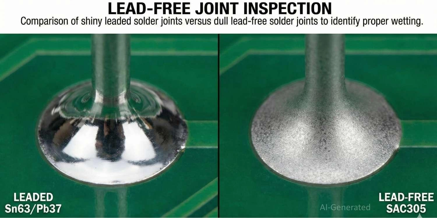
Figure: Comparison of shiny leaded solder joints versus dull lead-free solder joints to identify proper wetting.
Practical Tips for Using Flux in Lead-Free Soldering
● Tip Activator: Keep your iron tip tinned and use tip activator paste frequently, as lead-free solder oxidizes tips aggressively.
● Don't Crank the Heat: It is tempting to raise the iron temperature (>400°C) to make lead-free solder flow faster, but this burns off flux instantly and damages the tip. Keep the iron between 350°C and 370°C and use a larger tip geometry (chisel/hoof) to transfer heat efficiently.
● Fume Management: Lead-free flux requires higher activation temperatures, generating more acrid smoke. Ensure your fume extractor is positioned close to the work area to protect your respiratory health.
Conclusion
Successful lead-free soldering depends far more on flux behavior than many technicians realize. Because SAC alloys operate at higher temperatures and oxidize rapidly, using a flux designed for lead-free conditions—and applying it correctly—is non-negotiable. From selecting thermally stable flux chemistry to working within a short activation window, every step influences wetting quality and long-term joint reliability.
By understanding how flux reacts under lead-free temperatures, applying it generously but precisely, and avoiding excessive dwell or overheating, you can achieve consistent, reliable joints without resorting to extreme temperatures. Mastering flux usage not only improves solder flow—it reduces rework, protects components, and significantly lowers the risk of cold solder joints in modern lead-free assemblies.
Popular Articles
• Common PCB Assembly Methods and Soldering Techniques Explained
• What Is BGA Void? Causes, IPC Limits, and Solutions
• SMD Soldering Tools You Need: Complete Guide from Beginner to Pro
• Reflow Soldering: Everything You Need to Know
• SMT Assembly Process Explained and Equipment Used: A Step-by-Step Guide to PCBA Manufacturing
Keep Learning
Common PCB Assembly Methods and Soldering Techniques Explained
Whether you're designing your first prototype or scaling up to production, understanding PCB assembly methods and soldering techniques is crucial to achieving reliable, high-performance circuit boards. Modern PCBA primarily relies on Surface Mount Technology (SMT) and Through-Hole Technology (THT)—each offering unique advantages for component density, durability, and manufacturability. In this guide, we'll break down the major PCB assembly methods, key soldering techniques such as reflow and wave sold......
12 Professional Soldering Tips and Tricks Every Beginner Should Know
Soldering is not merely "gluing" metal; it is a metallurgical process that creates an intermetallic compound (IMC). This molecular bond ensures the electrical and mechanical integrity of your device. A poor joint might pass a quick visual check but will inevitably fail under vibration or thermal stress, leading to "ghost" bugs and hardware failures. These soldering tips and tricks focus on practical, repeatable techniques used in professional electronics soldering—from correct heat transfer and flux u......
Solder Melting Point Guide: Chart, Alloy Types, and Reflow Considerations
In the precise world of electronics manufacturing, a difference of just a few degrees can mean the distinction between a perfect, reliable solder joint and a catastrophic "cold" joint failure. While many hobbyists view soldering simply as "melting metal to stick things together," professional PCB assembly requires a nuanced understanding of thermodynamics. The solder melting point is not simply a single value listed in a datasheet; it is a decisive limit that determines the choice of components, the s......
The Ultimate Guide to Solder Flux: Everything You Should Know Before Soldering PCB
Soldering is needed to make almost all electronic devices. Adding solder alone won't make a joint that is strong, clean, and sound from a metallurgical point of view. Solder flux is a very important part of the process that comes in here. If you want to do your job better and make it more reliable, you need to know a lot about soldering flux, whether you're an engineer, a professional technician, or just a hobbyist. This article goes into a lot of detail about solder flux, including what it is, how it......
Flex PCB Assembly Guide: Process, Challenges, and Solutions
Flexible Printed Circuit Boards (Flex PCBs) are the foundational technology enabling the compact, innovative design of modern electronics. Because of their ability to bend and fold, they power devices from smart wearables to compact medical instruments where traditional rigid printed circuit boards (Rigid PCBs) can't be used. Achieving a functional electronic circuit from the raw plastic film demands special expertise, with flexible PCB assembly (FPCA) representing the crucial final step in this trans......
SMD Rework Guide: Tools, Temperatures, and Techniques That Prevent PCB Damage
From replacing a burned regulator to correcting wrong component values or removing solder bridges on fine-pitch ICs, SMD rework is an essential skill in electronics manufacturing and prototyping. It allows engineers to repair assembly defects, implement design changes, and recover valuable PCBs without the cost and delay of building new boards. In this guide, you will learn: What SMD rework is Common rework scenarios Tools and temperatures Safe removal and installation Package-specific techniques Real......