
PIC16F877A Master Trainer Board: An All-In-One Learning Tool Supported by JLCPCB
9 min
- Introduction to the Design
- Key Obstacles Encountered
- Benefits from JLCPCB Services
- Detailed Engineering Insights
- Main Elements Breakdown
- Achieved Performance
- Feedback and Conclusion
- FAQ:
In the realm of embedded systems training and quick prototyping, a solid trainer board is key for mastering microcontroller skills and hardware integration. This feature highlights the creation of the PIC16F877A Master Trainer Project, a multifunctional board centered on Microchip's renowned 8-bit microcontroller. The PIC16F877A, part of Microchip's mid-range family, has been a staple in electronics education since its introduction in the late 1990s, offering a balance of performance, cost, and ease of use that makes it ideal for beginners and professionals alike. By utilizing JLCPCB's cutting-edge PCB production and assembly capabilities, the initiative delivered top-tier outcomes with rapid production cycles, enabling seamless iteration and deployment for educational and hobbyist purposes.
Introduction to the Design
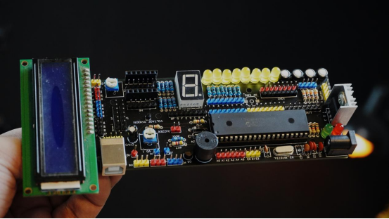
The PIC16F877A Master Trainer Board serves as a complete development environment featuring the PIC16F877A microcontroller, which boasts a RISC design, 8KB flash storage for program memory, 368 bytes of RAM for data handling, and 256 bytes of integrated EEPROM for non-volatile storage. It also includes advanced peripherals such as a 10-bit Analog-to-Digital Converter (ADC) with up to 8 channels, multiple timers for precise timing operations, Capture/Compare/PWM modules for motor control and signal generation, and communication interfaces like USART for serial communication, SSP for I2C/SPI, and parallel slave port. These features make it versatile for a wide range of applications, from simple LED blinking to complex sensor data acquisition and control systems.
The board incorporates diverse peripherals for practical training and testing, allowing users to experiment with real-world scenarios:
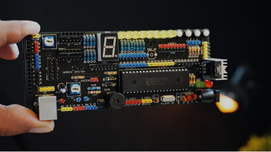
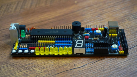
Core Chip: PIC16F877A in a 40-pin DIP format for straightforward coding, debugging, and component swaps, supporting in-circuit serial programming (ICSP) for quick firmware updates without removal.
Output Devices: A multiplexed 7-segment LED display for showing numeric values like counters or sensor readings, and a 16x2 LCD module for detailed textual feedback, such as status messages or debug information, configurable in 4-bit or 8-bit mode to optimize pin usage.
Controls and Signals: Multiple yellow LEDs for visual status indication (e.g., binary outputs or error alerts), tactile push buttons for user inputs like mode selection, DIP switches for configuring settings without code changes, and a potentiometer connected to a voltage divider for generating variable analog signals to test ADC functionality.
Sound and Detection: An active buzzer for audible notifications, such as alarms or feedback tones via PWM, plus dedicated ports for connecting external sensors like temperature (e.g., LM35), light (phototransistor), or humidity modules, enabling environmental monitoring projects.
Interfaces: Fully accessible I/O ports (Ports A through E) with color-marked pin headers for easy probing and expansion, a USB port for both power supply and programming via bootloader, and a DC input jack with onboard voltage regulation (including a heat sink for thermal management during high-load operations).
Extras: A built-in voltage splitting setup for reference voltages, a reset switch for quick restarts, and a 20MHz crystal oscillator for high-precision clocking, ensuring reliable operation in time-sensitive applications.
Sized at about 15cm by 5cm, it's portable while packed with features suitable for teaching fundamental concepts like interrupt handling, peripheral configuration, and firmware development. This design draws inspiration from popular trainer kits, making it an excellent platform for students to transition from theory to practice in embedded programming using tools like MPLAB IDE or XC8 compiler.
Key Obstacles Encountered
Building this trainer board involved multiple difficulties, particularly in balancing functionality with usability:
Layout Complexity: Fitting over 50 components, both through-hole (THT) and surface-mount (SMD) types—including resistors for pull-ups, capacitors for decoupling, LEDs for indicators, and various connectors—onto a single or dual-layer PCB while maintaining clear silkscreen markings, logical grouping of modules, and user-friendly access to prevent accidental shorts or misconnections during experiments.
Durability for Training: Ensuring the board could handle frequent use, such as repeated flashing of firmware (potentially hundreds of times in a classroom setting), exposure to static discharge, and possible mishaps by beginners like reversed polarity or overvoltage, which demanded reinforced traces, ESD protection diodes, and superior soldering quality to avoid cold joints or failures.
Budget and Speed: Obtaining components affordably and building samples swiftly for low-volume prototype runs, without sacrificing placement accuracy for tight-spaced parts like the MCU's 0.1-inch pin leads or fine-pitch SMD resistors, all while adhering to educational budget constraints and tight project timelines.
Additional challenges included thermal management for the voltage regulator during extended demos and signal integrity for high-speed peripherals, which required careful trace routing to minimize noise and crosstalk.
Benefits from JLCPCB Services
JLCPCB's all-inclusive offerings played a crucial role in addressing these issues, providing a seamless workflow from design to delivery. The project leveraged JLCPCB's PCB fabrication services for precise milling, multi-layer support, and high-resolution silkscreen labeling to enhance usability. This was paired with their SMT assembly for efficient placement of surface elements, reducing manual labor and errors. Notable aspects include:
Available Inventory: Standard items like 1% tolerance resistors, ceramic capacitors, high-brightness LEDs, and the PIC16F877A microcontroller itself were sourced directly from JLCPCB's extensive in-house library of over 200,000 parts, guaranteeing compatibility, RoHS compliance, and eliminating supply chain holdups that could delay prototyping.
Dual-Side Placement: Automated SMT lines managed precise positioning and soldering on both board faces, handling components as small as 0402 packages, while through-hole support was available via optional hand assembly or wave soldering for larger parts like the DIP MCU and pin headers.
Manufacturing Readiness Check: Initial design reviews using JLCPCB's free DFM (Design for Manufacturability) tools identified potential issues like insufficient clearances or via placements, allowing optimizations before production. The use of ENIG (Electroless Nickel Immersion Gold) surface finish ensured enhanced solder adhesion, corrosion resistance, and longevity, ideal for boards subjected to frequent handling.
This unified approach not only simplified the process from Gerber file and BOM submission to fully assembled boards but also incorporated quality enhancements like impedance control for better signal performance and optional functional testing. JLCPCB's economies of scale kept costs low, making it feasible for small-batch educational projects.
Detailed Engineering Insights
Hardware Specs
| Parameter | Details |
| Layers | 2 (FR-4 material with 1.6mm thickness for robustness) |
| Dimensions | 150mm x 50mm |
| Finish | ENIG for corrosion resistance and flat soldering surfaces |
| Components | 50+ (mix of SMD and THT, including passive and active elements) |
| Power | 5V regulated output via USB or 7-12V DC jack with LM7805 regulator and heat sink for up to 1A draw |
Main Elements Breakdown
Processing Unit: The PIC16F877A is paired with a 20MHz crystal oscillator and 22pF loading capacitors for swift performance, enabling instruction cycles as fast as 200ns and supporting applications requiring real-time responses.
Interaction Features: The 7-segment display is driven directly by port pins with current-limiting resistors, while the LCD is interfaced in 4-bit or 8-bit mode, allowing for custom character generation and backlight control.
Add-Ons: Buzzer connected to a PWM-capable pin for variable tone generation (e.g., melodies or alerts), and the potentiometer routed to an ADC channel for precise voltage sensing, demonstrating analog-to-digital conversion principles.
Energy Handling: The onboard regulator with a heat sink supports up to 1A, providing a stable 5V rail with bypass capacitors to filter noise, crucial for sensitive analog operations.
The build sequence was meticulously planned:
1. Application of solder paste using stencils for SMD components.
2. Robotic pick-and-place machines for high-precision component placement.
3. Controlled reflow soldering in convection ovens to form reliable joints.
4. Manual fitting and wave soldering for through-hole items like the DIP microcontroller, connectors, and larger capacitors.
JLCPCB's rigorous inspections, including Automated Optical Inspection (AOI) for defects like bridging or misalignment, X-ray for hidden solder joints, and functional testing options, guaranteed flawless final products ready for immediate use.
Achieved Performance
Five test units arrived in just 5 days, fully assembled, visually inspected, and functionally verified. Upon activation and initial programming:
All displays and LEDs operated properly, with the 7-segment successfully running demo patterns like counting sequences, and the LCD displaying scrolling text without artifacts.
Sensor interfaces and the buzzer responded as intended, producing clear tones and accurately reading analog inputs with minimal noise.
Power stability and signal integrity remained consistent during prolonged sessions, even under varying loads, with no overheating issues thanks to the heat sink.
The units excelled in training sessions, supporting effortless USB-based coding and debugging, and proved robust in hands-on workshops where participants built projects like digital thermometers or traffic light controllers. Long-term testing showed no failures after hundreds of cycles, validating the design's durability.
Feedback and Conclusion
JLCPCB's integrated platform simplifies complex PCB development by handling fabrication, sourcing, and assembly, accelerating time-to-market and shifting focus to innovation. Emphasizing DFM early on minimizes revisions and costs, particularly for educational trainer boards with limited budgets. The PIC16F877A's versatility excels in teaching and applications like automation, robotics, and controls, enhanced by reliable manufacturing. Overall, this project demonstrates how affordable production democratizes embedded learning, inspiring future engineers.

FAQ:
1.Why opt for ENIG coating here?
It offers smooth, bondable areas perfect for hybrid SMD/THT builds and enduring use in training environments, preventing oxidation and ensuring reliable connections over time.
2.How does JLCPCB manage through-hole parts?
While focused on SMT for efficiency, they provide THT assembly options, including manual insertion and wave soldering, for complete PCBA solutions in mixed-technology boards.
3.Is replication possible?
Absolutely! Share designs on open-source platforms like OSHWLab or GitHub, and JLCPCB handles Gerber files and BOM uploads for simple, cost-effective ordering of duplicates or variants.
4.What about tailored additions?
Their adaptable services support customizations, such as adding more layers for complex routing, advanced finishes like hard gold for connectors, or even full turnkey assembly with custom enclosures.

Popular Articles
• PiBrick Pocket-CM5: A Compact Raspberry Pi CM5 Handheld PC Built with JLCPCB
• From Membrane Frustration to Custom Mechanical Mastery: Taifur's V3 Full Keyboard Project
• Turn Your Raspberry Pi Pico into a Professional JTAG Programmer with DirtyJTAG & OpenFPGALoader
• Premium Portable Speaker Built with 8-Layer PCBs, DSP & Smart Amps
• ESP32 Smart Control Board for Realistic RC Model Automation
Keep Learning
PiBrick Pocket-CM5: A Compact Raspberry Pi CM5 Handheld PC Built with JLCPCB
Key Takeaways The piBrick Pocket-CM5 is a fully functional, smartphone-sized Raspberry Pi CM5 handheld PC with a physical QWERTY keyboard, AMOLED display, and M.2 NVMe SSD The project utilizes JLCPCB's 4-layer PCB fabrication with controlled impedance (90-ohm for USB, 100-ohm for PCIe/MIPI DSI) to maintain signal integrity Designed using EasyEDA and fabricated by JLCPCB, the project was submitted to the EasyEDA Spark program, successfully securing parts and materials sponsorship for its development. J......
From Membrane Frustration to Custom Mechanical Mastery: Taifur's V3 Full Keyboard Project
Note Motivation: Replaced a dust-prone membrane keyboard with a durable, custom DIY alternative. Specs: 87-key TKL layout powered by Raspberry Pi Pico (RP2040), featuring hot-swap support, QMK, OLED, and an encoder. Design: A unique 3-layer PCB stack featuring symmetrical routing, an exposed controller, and visible "diode art". Support: Designed using EasyEDA and fabricated by JLCPcB, the project was submitted to the EasyEDA Spark program successfully securing parts and materials sponsorship for its d......
ESP32 Smart Control Board for Realistic RC Model Automation
Key Takeaways This project demonstrates how a well-designed custom PCB, manufactured and assembled through JLCPCB, can democratize advanced electronics for hobbyists. Key lessons include: Prioritizing compact, high-density layouts while respecting DFM rules. Leveraging professional SMT assembly for complex boards. Designing with clear labeling and modularity for user-friendliness. Choosing a manufacturing partner whose capabilities match your project's needs for consistent results. Project Overview: B......
Premium Portable Speaker Built with 8-Layer PCBs, DSP & Smart Amps
Project Background and Introduction When you unbox a beautifully crafted portable speaker that delivers rich, room-filling sound with crisp highs, deep bass, and intelligent audio processing, it’s easy to imagine it came from a big-name factory. But behind this elegant Harman/Kardon-inspired design lies the story of an innovative maker who turned a personal passion project into a fully functional, high-performance audio system—entirely prototyped and produced with JLCPCB’s PCB and PCBA services. This ......
Turn Your Raspberry Pi Pico into a Professional JTAG Programmer with DirtyJTAG & OpenFPGALoader
In the world of FPGA development, having a reliable, low-cost JTAG programmer used to mean either buying expensive vendor cables or adding high-cost FTDI chips to every board. Maker Khaled Magdy changed that by turning a $4 Raspberry Pi Pico into a fully functional JTAG adapter using DirtyJTAG firmware and OpenFPGALoader — then had his custom FPGA boards professionally assembled by JLCPCB. The entire solution is 100% open-source. You can download the firmware, follow the Windows installation steps, an......
Build a Professional 8x8 RGB LED Matrix with JLCPCB
In the world of DIY electronics, building a clean, reliable 8×8 RGB LED matrix used to mean hours of painstaking hand-soldering — 64 WS2812B LEDs plus 64 decoupling capacitors. That all changed when maker Lucas Fernando designed a fully custom PCB from scratch and had it professionally assembled by JLCPCB on his very first try. The result? Five perfectly finished, ready-to-use 8×8 addressable LED matrices that look like commercial products. Best of all, the entire project is 100% open-source. You can ......