
How to Use Solder Flux for SMD Rework and Repair (Step-by-Step)
5 min
- Step-by-Step: How to Use Solder Flux for SMD Rework
- Practical Tips for Using Flux During SMD Rework
- Conclusion
Correct flux use is critical for SMD rework and repair. This guide answers key questions, shows step-by-step techniques, and shares practical tips to ensure reliable solder joints.
Before getting into the step-by-step process, let’s answer the most common practical questions asked when using solder flux for SMD rework and repair.
Q1: Should You Always Apply Flux Before Desoldering?
Yes. Applying flux before desoldering helps transfer heat from the iron/hot air to the solder joint faster, reducing the thermal stress on the component and the PCB pad.
Q2: Should You Reapply Flux During SMD Rework?
Absolutely. Once the old component is removed, the old flux is spent. You must clean the area and apply fresh flux before placing the new component to ensure a good bond.
Q3: Which Flux Should You Use for Sensitive Components?
Use No-Clean (NC) or Rosin Mildly Activated (RMA) gel flux. Avoid Water-Soluble (OA) flux for rework unless you can wash the board immediately, as residues trapped under the component can cause corrosion.
Q4: Where Should You Apply Flux During SMD Rework - Pads, Leads, or Both?
Apply flux primarily to the pads on the PCB. If reusing a component, you may also flux the leads/balls.
Q5: How Much Flux Is Too Much During Rework?
Excess flux can boil under the component during hot air reflow, causing the part to "popcorning" or shift out of alignment. Use just enough to coat the pads.
Q6: Can Flux Damage Pads or PCB During Rework?
Flux itself generally doesn't damage pads, but flux exhaustion leads to overheating. If the flux burns off and you keep applying heat, you risk lifting the pads. Keeping fresh flux on the joint protects the pad.
Step-by-Step: How to Use Solder Flux for SMD Rework
1. Thermal Coupling for Removal: Apply a liberal amount of flux to the existing component joints. Before applying hot air, this flux acts as a thermal bridge, transferring heat from the nozzle to the solder alloy efficiently. Without flux, the hot air oxidizes the joints further, requiring higher temperatures to achieve melt (liquidus).
2. Site Remediation (Wicking): Once the component is removed, apply fresh tacky flux over the residual solder on the pads. Use a desoldering braid (wick) to remove the old alloy. Crucial: Never use dry wick on a dry pad; the friction will lift the copper traces. The flux lubricates the wick and ensures the old solder flows into the braid instantly. Clean the area thoroughly with IPA to remove charred residues.
3. Controlled Flux Deposition: Apply a very thin film of Tacky Gel Flux to the clean pads. Do not use liquid flux here, as it will evaporate before the new component is placed. The goal is to provide just enough tackiness to hold the component in place against the airflow, but not enough to cause it to "float" or skew.
4. Reflow & Self-Alignment: Place the new component on the fluxed pads. Apply hot air at a low airflow setting. As the flux activates, it cleans the pads and leads. When the solder paste (or pre-tinned pads) reaches melting point, the high surface tension of the molten solder - facilitated by the flux - will pull the component into perfect alignment with the pads (the "self-alignment mechanism").
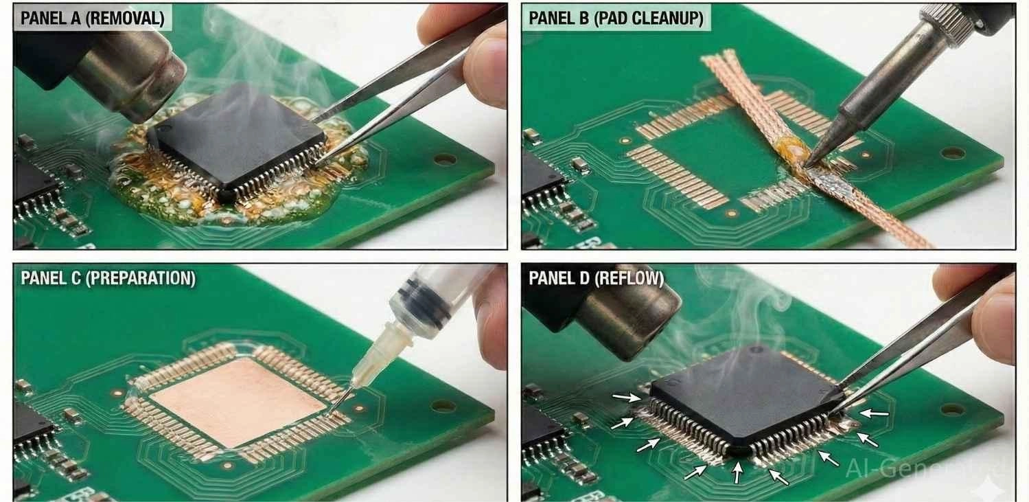
Figure: Step-by-step visual guide for SMD rework: fluxing for removal, cleaning pads with wick, fluxing for placement, and hot air reflow.
Practical Tips for Using Flux During SMD Rework
● Use Gel Flux: Liquid flux evaporates too fast under hot air. Gel stays active longer.
● Ventilation: Rework generates significant smoke; ensure good airflow.
● Shield Neighbors with Kapton Tape: Flux splatter and heat can affect adjacent components. Cover surrounding areas with polyimide (Kapton) tape to create a thermal and chemical shield.
● Avoid the "Floating" Effect: Do not create a pool of flux. If the layer is too thick, the component will "surf" on the boiling flux and skew off the pads. Use a thin film only.
● Clean Before New Application: Always clean charred old flux with IPA before adding fresh flux. Layering new flux over burnt residue creates a thermal barrier that hinders heat transfer.
● Preheat the Area Slightly: Warm the pads slightly before applying hot air. This reduces thermal shock and helps flux activate evenly.
● Use Minimal Airflow: Keep hot air speed low to avoid blowing small components off the pads during reflow.
● Angle the Nozzle Correctly: Position the hot air nozzle at ~45° to the board. This improves heat transfer while minimizing flux splatter.
● Avoid Cross-Contamination: Use a dedicated brush or applicator for flux. Don’t touch fluxed pads with tweezers that handled other components.
● Monitor Flux Color Changes: Some fluxes darken as they reach activation temperature. Use this as a visual cue for proper heating.
Conclusion
Proper flux application is essential for safe and reliable SMD rework and repair. Using the right type of flux, applying it evenly, and controlling heat and airflow helps prevent pad damage and component misalignment.
Following practical tips—such as preheating pads, angling the hot air nozzle correctly, and monitoring flux activation—ensures consistent solder flow, strong joints, and long-term board reliability.
Popular Articles
• Common PCB Assembly Methods and Soldering Techniques Explained
• What Is BGA Void? Causes, IPC Limits, and Solutions
• SMD Soldering Tools You Need: Complete Guide from Beginner to Pro
• Reflow Soldering: Everything You Need to Know
• SMT Assembly Process Explained and Equipment Used: A Step-by-Step Guide to PCBA Manufacturing
Keep Learning
12 Professional Soldering Tips and Tricks Every Beginner Should Know
Soldering is not merely "gluing" metal; it is a metallurgical process that creates an intermetallic compound (IMC). This molecular bond ensures the electrical and mechanical integrity of your device. A poor joint might pass a quick visual check but will inevitably fail under vibration or thermal stress, leading to "ghost" bugs and hardware failures. These soldering tips and tricks focus on practical, repeatable techniques used in professional electronics soldering—from correct heat transfer and flux u......
Solder Melting Point Guide: Chart, Alloy Types, and Reflow Considerations
In the precise world of electronics manufacturing, a difference of just a few degrees can mean the distinction between a perfect, reliable solder joint and a catastrophic "cold" joint failure. While many hobbyists view soldering simply as "melting metal to stick things together," professional PCB assembly requires a nuanced understanding of thermodynamics. The solder melting point is not simply a single value listed in a datasheet; it is a decisive limit that determines the choice of components, the s......
The Ultimate Guide to Solder Flux: Everything You Should Know Before Soldering PCB
Soldering is needed to make almost all electronic devices. Adding solder alone won't make a joint that is strong, clean, and sound from a metallurgical point of view. Solder flux is a very important part of the process that comes in here. If you want to do your job better and make it more reliable, you need to know a lot about soldering flux, whether you're an engineer, a professional technician, or just a hobbyist. This article goes into a lot of detail about solder flux, including what it is, how it......
Common PCB Assembly Methods and Soldering Techniques Explained
Whether you're designing your first prototype or scaling up to production, understanding PCB assembly methods and soldering techniques is crucial to achieving reliable, high-performance circuit boards. Modern PCBA primarily relies on Surface Mount Technology (SMT) and Through-Hole Technology (THT)—each offering unique advantages for component density, durability, and manufacturability. In this guide, we'll break down the major PCB assembly methods, key soldering techniques such as reflow and wave sold......
Flex PCB Assembly Guide: Process, Challenges, and Solutions
Flexible Printed Circuit Boards (Flex PCBs) are the foundational technology enabling the compact, innovative design of modern electronics. Because of their ability to bend and fold, they power devices from smart wearables to compact medical instruments where traditional rigid printed circuit boards (Rigid PCBs) can't be used. Achieving a functional electronic circuit from the raw plastic film demands special expertise, with flexible PCB assembly (FPCA) representing the crucial final step in this trans......
SMD Rework Guide: Tools, Temperatures, and Techniques That Prevent PCB Damage
From replacing a burned regulator to correcting wrong component values or removing solder bridges on fine-pitch ICs, SMD rework is an essential skill in electronics manufacturing and prototyping. It allows engineers to repair assembly defects, implement design changes, and recover valuable PCBs without the cost and delay of building new boards. In this guide, you will learn: What SMD rework is Common rework scenarios Tools and temperatures Safe removal and installation Package-specific techniques Real......