
How to Prevent Solder Balls in PCB Assembly: A Complete Guide
9 min
- What Are Solder Balls in PCB Assembly?
- Causes of Solder Ball Formation
- How SMT Stencil Design Directly Influences Solder Balling?
- Professional Strategies to Eliminate Solder Balls During Assembly
- Why JLCPCB Stencils Are the Standard for Reliable PCB Assembly?
- Final Thoughts:
- Q: What is the difference between a solder ball and a solder bead?
- Q: How many solder balls are allowed per IPC-A-610?
- Q: Can I reuse solder paste left on the stencil?
- Q: Does nitrogen (N₂) reflow reduce solder balling?
- Q: What do tombstoning and solder balls both appearing indicate?
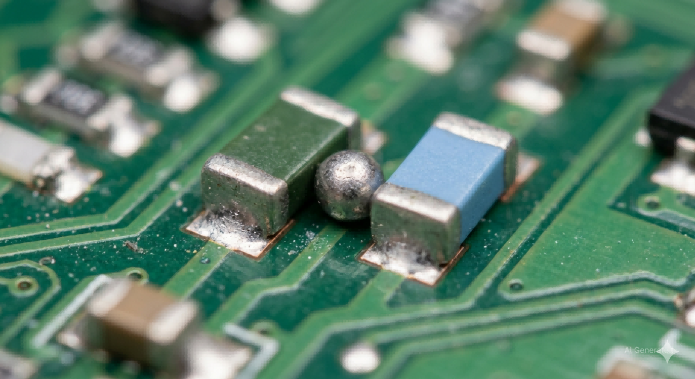
Take one of the boards off the line, and put it under the microscope, and there they are, little metallic balls here and there on the solder mask. This is one of the reasons why solder balls are dangerous, because they do not lead to immediate failure.
A ball sitting clear of any conductor looks harmless until the product vibrates, thermally cycles, and the ball migrates into a gap between two traces. Six months later: an intermittent fault with no obvious cause. They're also a process signal where consistent balling means something has drifted.
This guide covers what IPC-A-610 defines, what physically causes them, how stencil design drives or prevents them, and the practical steps to keep them off boards.
What Are Solder Balls in PCB Assembly?
IPC-A-610 defines solder balls as small spheres of solder separated from the main pool during reflow, ejected or stranded particles that ended up somewhere unintended.
Usually, the non-conformance begins at diameters over 0.13 mm, or more than five per 600 mm². Even in-spec balls are a latent short circuit on high-density boards. It's when mechanical stress moves them.
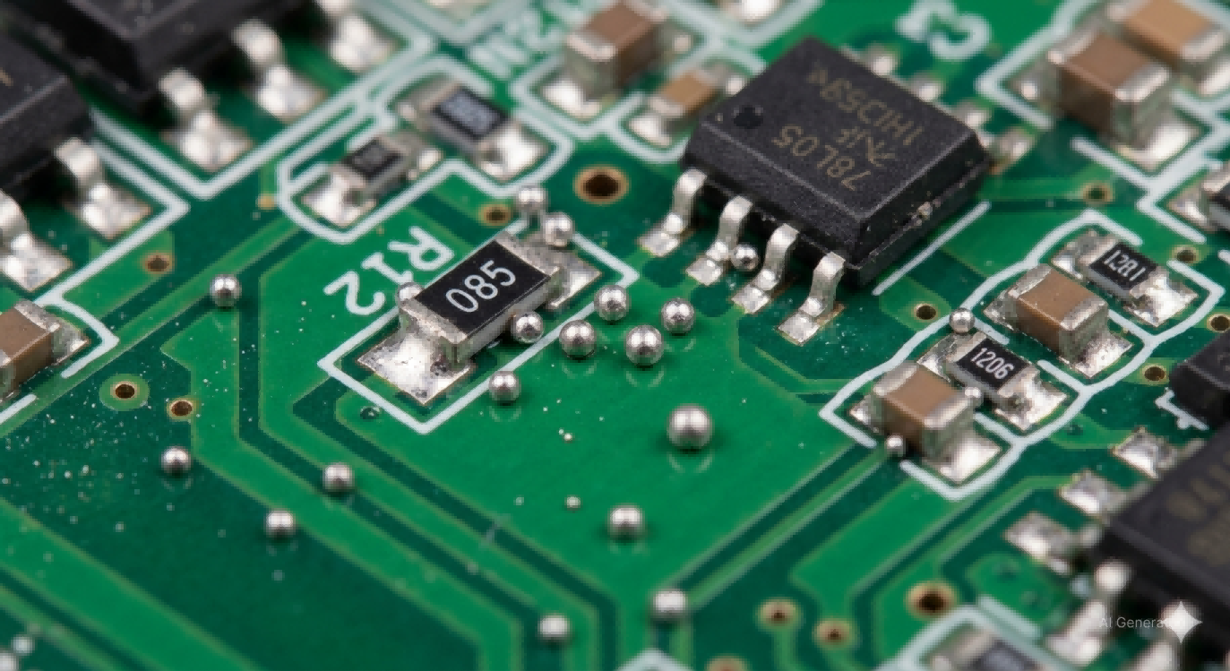
The typical location of these defects is variable. Sometimes there are balls under chip components, indicating paste slump. Or sometimes there are balls near via barrels that indicate outgassing. And fine balls scattered broadly suggest moisture.
Causes of Solder Ball Formation
Five root causes cover most solder ball defects, and on real lines, they stack. Slightly oxidised paste combined with an aggressive ramp rate produces far more balling than either problem alone.
Solder Paste Slump:
Paste is thixotropic, that is, it flows under squeegee pressure and hardens when at rest. Cold slump happens at room temperature due to low viscosity or humidity uptake.
Hot slump is worse in the pre-heat zone, the paste softens before flux activates, and spreads onto the solder mask. And when wetting, it pulls the main mass back onto the pad. Stranded particles on the mask have nowhere to bond and solidify as solder balls.
Oxidation:
Flux must reduce metal oxides on solder powder and PCB pads before reaching the liquidus, which is approximately 217°C for SAC305.
When the oxide burden is too high, aged paste, degraded OSP, boards stored past shelf life, flux exhausts itself before coalescence completes, leaving unfused particles as independent balls. ENIG handles this far better than OSP, as the table below shows:
PCB Pad Finish: Oxidation and Solder Ball Risk Comparison
| Finish | Solderability | Oxidation Risk | Solder Ball Risk |
| HASL (Sn/Pb) | Excellent | Low | Low |
| Lead-Free HASL | Good | Low–Medium | Low–Medium |
| ENIG | Excellent | Very Low | Very Low |
| OSP | Good (short shelf) | Medium–High | Medium–High |
| Immersion Ag | Very Good | Low (tarnish risk) | Low |
| Immersion Sn | Good | Medium | Medium |
Moisture:
Moisture that is present is suddenly vaporised in the oven, and the solder particles are ejected, thus physically, before they are attached to the joint using flux. The pattern is distinctive: fine balls scattered broadly across the board rather than clustered near specific pads.
Reflow Profile Errors:
Ramp rates above 2°C/s through pre-heat cause solvent evaporation violent enough to carry solder particles with it. An insufficient soak phase at 150–200°C, where the flux removes oxides, means the solder reaches the liquidus before coalescence conditions are met.
Both problems are confirmed only with a thermal profiler on the actual board, not the oven controller.
Poor Paste Printing:
Excessive squeegee pressure smears paste across the solder mask between pads, isolated deposits with no metallic surface to wet. They ball up in the oven right where they sit. A worn stencil compounds it: ragged aperture walls create torn deposits that transfer smears to subsequent boards.
How SMT Stencil Design Directly Influences Solder Balling?
The stencil defines every paste deposit on the board. Get the aperture geometry wrong, and downstream fixes become compensations rather than solutions.
Area Ratio:
Area Ratio = aperture opening area ÷ aperture wall area, and it must exceed 0.66 for reliable paste release. Below that threshold, adhesion to the walls wins the deposit tears on stencil separation, leaving fragments that become solder balls.
Mixed-technology boards often need step stencils precisely because no single foil thickness satisfies the area ratio for every pad simultaneously.
Aperture Reduction and Shape:
Sizing apertures 10–20% smaller than the pad buffers against placement-induced paste displacement. For passives, shape matters: home-plate apertures taper toward the component body, concentrating paste at pad extremities and away from the centre where squeeze-out occurs.
Bow-tie and U-shapes serve the same purpose on progressively smaller components.
Wall Smoothness:
Rough walls cause dog-earing deposit corners tear on stencil lift, stick to the underside, and transfer back to boards as isolated solder mask smears.
Electropolished stencils remove microscopic wall irregularities; nano-coated stencils add a hydrophobic layer that actively repels paste. Both reduce deposit variation and underside cleaning frequency.
Precision stencil services make sure they are using the right aperture design. Because that's where it all starts.
Professional Strategies to Eliminate Solder Balls During Assembly
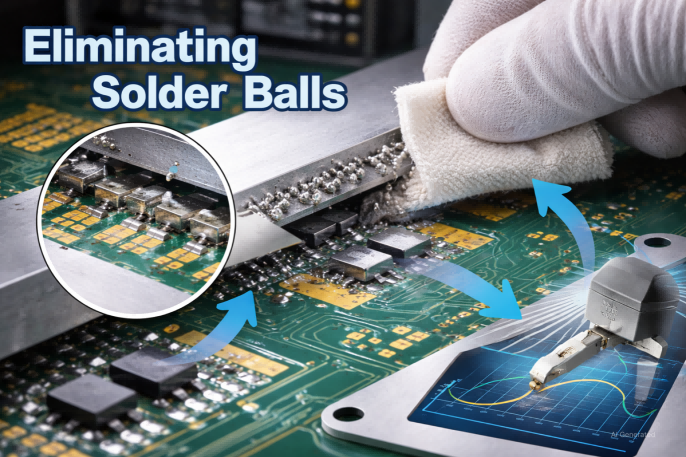
Prevention is cheaper than rework. Most solder ball problems are fixed before the board enters the oven. Here are the golden rules to eliminate solder balls.
● Store paste at 3–10°C. Warm sealed cartridges to room temperature for 4 hours before opening. Opening cold causes condensation directly on the paste surface.
● Hold SMT room humidity at 40–60% RH. Above 60%, printed boards absorb moisture within hours.
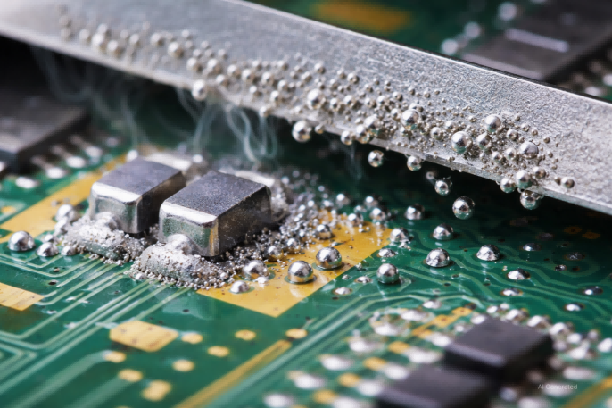
● Wipe the stencil underside every 3–5 prints with IPA solvent. Fine-pitch work warrants every print.
● Reflow within 1 hour of printing. Beyond 2 hours, clean and reprint.
● Profile the board with a thermal probe, not the oven controller. Confirm ramp rate stays under 2°C/s and soak duration matches the board's thermal mass.
● Audit pick-and-place nozzle force on small passives. Bottoming into the paste deposit squeezes material outward on every cycle.
Why JLCPCB Stencils Are the Standard for Reliable PCB Assembly?
Stencil quality determines paste deposit quality. There's no downstream compensation for dimensional variability introduced at the print stage. And that's where JLCPCB comes in with their top-tier stencil production.
High-precision technology
For starters, they ensure exceptional accuracy of up to ±0.003 mm using 30 high-precision LPKF laser cutting machines. It guarantees compliance with area ratios even on 0.4 mm pitch pads.
Premium Materials and Durability
Almost every stencil from JLCPCB comes with a durable 304 HTA stainless steel build. With this material, you can easily expect impeccable hardness and thermal stability. No worries of facing deformities even after multiple printing cycles.
Advanced Finishing Options
JLCPCB offers advanced post-processing options like -
● Electropolishing: This finishing process ensures smoother aperture walls. It also removes any kind of micro burrs of slag left from laser cutting.
● Nano-Coating: A Nano-coating finish makes the stencil ideal for PCBs that have BGA, QFN, or different fine-pitch components. It’s great for higher SMT first pass yield.
Versatile Customization
JLCPCB supports a wide range of custom requirements. You can choose between framed stencils for automated machines or frameless versions for manual assembly.
● Step Stencils: These involve localized "step-up" or "step-down" thickness on one sheet. This guarantees fine-pitch and large-scale components of the correct volume of paste needed to have high-quality joints on mixed-technology boards.
● Fiducials: JLCPCB offers three different fiducial options. For a perfect alignment, you can define etched through or half-etched fiducials.
Other than these, you get plenty of customization options.
Fast Turnaround and Affordability
Reliability is not at a high cost. Tailor-made stencils begin at $3. The automated production line has a build time of up to 12 hours. The majority of the orders are shipped within 24 hours, that keep your project on schedule. Stop solder balling with high-precision SMT stencils from JLCPCB. Claim your $11 coupon now and upgrade your assembly quality today!
Final Thoughts:
Solder balls are preventable. The physics of each failure mode is well understood, and every root cause responds to process discipline, paste storage, room environment, stencil condition, and profile verification.
None of it requires capital investment. When balls do appear, their location on the board is diagnostic information: use it before reaching for the rework iron.
Ensuring a clean assembly starts with high-fidelity tooling. In case you are scaling production, you can learn more about our JLCPCB stencils that can work as a solution to counter these frequent reflow defects.
Frequently Asked Questions:
Q: What is the difference between a solder ball and a solder bead?
A solder ball is a free-standing sphere ejected away from the joint with no metallic bond to anything. A solder bead is larger and elongated, physically attached to a chip component termination caused by paste squeezed out during placement and reflowed against the end-cap. Both fail IPC-A-610 when they are in violation of electrical clearance; however, the corrective actions are different, addressing stencil and profile issues, beading points, placement force, and aperture shape.
Q: How many solder balls are allowed per IPC-A-610?
To a maximum of five per 600 mm 2, with a diameter of 0.13 mm or less, so long as they are encapsulated or free of the smallest electrical clearance. Exceed any one condition, and it's a non-conformance. Most mature lines treat two or three per 600 mm² as a process flag rather than waiting for the IPC limit.
Q: Can I reuse solder paste left on the stencil?
Within limits. Most manufacturers specify 4–8 hours maximum on-stencil life. Paste recovered within that window, tested for viscosity, and refrigerated, sealed can be reused. Paste left overnight, visibly dried at the edges, or exposed to humidity above 60% RH should be discarded.
Q: Does nitrogen (N₂) reflow reduce solder balling?
Yes. Nitrogen holds oven oxygen below 100 ppm, so solder powder isn't re-oxidising during ramp and soak while the flux is trying to clean it. Flux completes oxide reduction with capacity to spare, coalescence is more complete, and fewer satellite particles remain. The most pronounced benefit is with SAC305 and other lead-free alloys. The trade-off is the nitrogen operating cost.
Q: What do tombstoning and solder balls both appearing indicate?
Tombstoning needs unequal wetting forces, usually unequal paste volumes on the two pads. When solder balls also appear, those deposits are poorly contained, spreading onto the solder mask. Together, they point strongly at a stencil problem or excessive squeegee pressure rather than a profile issue. Check print quality with a 3D SPI system before touching the oven.
Keep Learning
Manual Pick and Place: A Cost-Effective SMT Alternative
Key Takeaways for Manual Pick and Place Manual pick and place uses a hand-held vacuum wand and positioning stage to place SMD components by hand, replacing tweezers in prototype assembly. It is most cost-effective for production runs of 1 to 50 boards, where an automated SMT pick-and-place machine cannot justify its $10,000+ setup cost. A complete manual workstation runs $300 to $500, compared with $10,000+ for an entry-level automated pick and place machine. SMT stencil quality is the single largest ......
Hot Air Surface Mount Soldering: A Step-by-Step Guide
Key Takeaways Heat Control Is Everything: Hot air SMD soldering delivers uniform heat across all pads simultaneously, eliminating the lifted pads and cold joints common with iron-based soldering of fine-pitch components. Airflow Kills Small Parts: Set airflow to just 10–20% for 0402/0201 passives to avoid the Bernoulli Effect that turns tiny resistors into projectiles. Stencil Precision Prevents Tombstoning: A precision-cut SMT stencil deposits equal paste volume on both pads, balancing surface tensio......
Solder Paste Printing Defects: How Precision Stencils Prevent Assembly Failures
Key Takeaways 70% Rule: Approximately 70% of SMT defects originate from the solder paste printing stage, making it the most critical process to optimize. Root Causes: Defects like bridging, insufficient paste, misalignment, and slumping are caused by stencil tension, process parameters (pressure, speed), and paste chemistry/environment. Area Ratio Matters: Maintaining an aperture Area Ratio (AR) above 0.66 (per IPC-7525) is essential to ensure proper paste transfer efficiency and prevent chronic insuf......
Best Manual Pick and Place Tools for Precise PCB Assembly
While fully automated robotic SMT lines handle mass production efficiently, every hardware innovation begins on a workbench. Engineers shifting from soldering large through-hole components to microscopic surface-mount devices (SMD) by hand quickly realize that precision and control are everything. Achieving factory-level assembly on your desk is absolutely possible with the right setup. This guide reviews the essential tool categories needed to build an effective prototyping workbench, covering precis......
How to Use a BGA Stencil for SMT Assembly and Reballing (Design & Process Guide)
Anyone who's spent time in a lab knows the look. You flip over a BGA chip and stare at the bottom. Flat. Featureless. No legs. No leads. Just a grid of tiny silver bumps. First thought? How the hell am I supposed to solder this? The Ball Grid Array (BGA) package is a trade-off. You get insane I/O density in a tiny footprint. But every single connection is hidden. You can't see them, and you can't poke them with an iron. Here's the thing I learned after lifting more pads than I'd like to admit: learnin......
Solder Bead Prevention: How PCB Stencil Design & Process Control Deliver Defect-Free Reflow Soldering
In modern SMT assembly, solder joint quality is determined long before the reflow oven starts—at the solder paste printing stage. When this step is not properly controlled, the consequences appear after reflow as tiny spherical solder particles scattered around component pads: solder beads. For engineers working with high-density assemblies, these defects are familiar and frustrating because they reappear whenever a process variable drifts outside its optimum range. This guide takes an engineering-fir......