
Cold Solder Joint: The Complete Engineering Guide to Causes, Detection, and Prevention
11 min
- What Is a Cold Solder Joint?
- What Does a Cold Solder Joint Look Like?
- Why Cold Solder Joints Are Dangerous?
- What Causes a Cold Solder Joint?
- How to Identify a Cold Solder Joint
- How to Fix a Cold Solder Joint
- How to Prevent Cold Solder Joints in PCB Assembly
- Cold Solder Joint vs Other Solder Defects
- Industry Standards Related to Cold Solder Joints
- Conclusion
- FAQs about Cold Solder Joint
Cold solder joints are one of the most common — and most dangerous — soldering defects in PCB assembly.
They often look harmless, but can cause intermittent failures, unexpected resistance spikes, and field returns long after a product has passed initial testing. In vibration-prone or thermally stressed environments, a single cold joint can bring down an entire system.
This guide explains what a cold solder joint is, what it looks like, why it happens, and how to reliably identify, fix, and prevent it. Whether you’re troubleshooting a failed board or optimizing an SMT production line, this article gives you a practical, engineering-level reference for eliminating cold solder joints and improving long-term reliability.
What Is a Cold Solder Joint?
Technically, a cold solder joint occurs when the solder does not melt completely or the surface being soldered has not reached the liquidus temperature of the alloy.
In a proper solder joint, the solder enters a liquid phase, wets the pad and component lead, and facilitates atomic diffusion to create an IMC layer. In a cold solder joint, this wetting is incomplete. The solder sits "on top" of the pad rather than bonding "with" it. This results in a connection that may conduct electricity initially but suffers from extremely high resistance and mechanical brittleness.
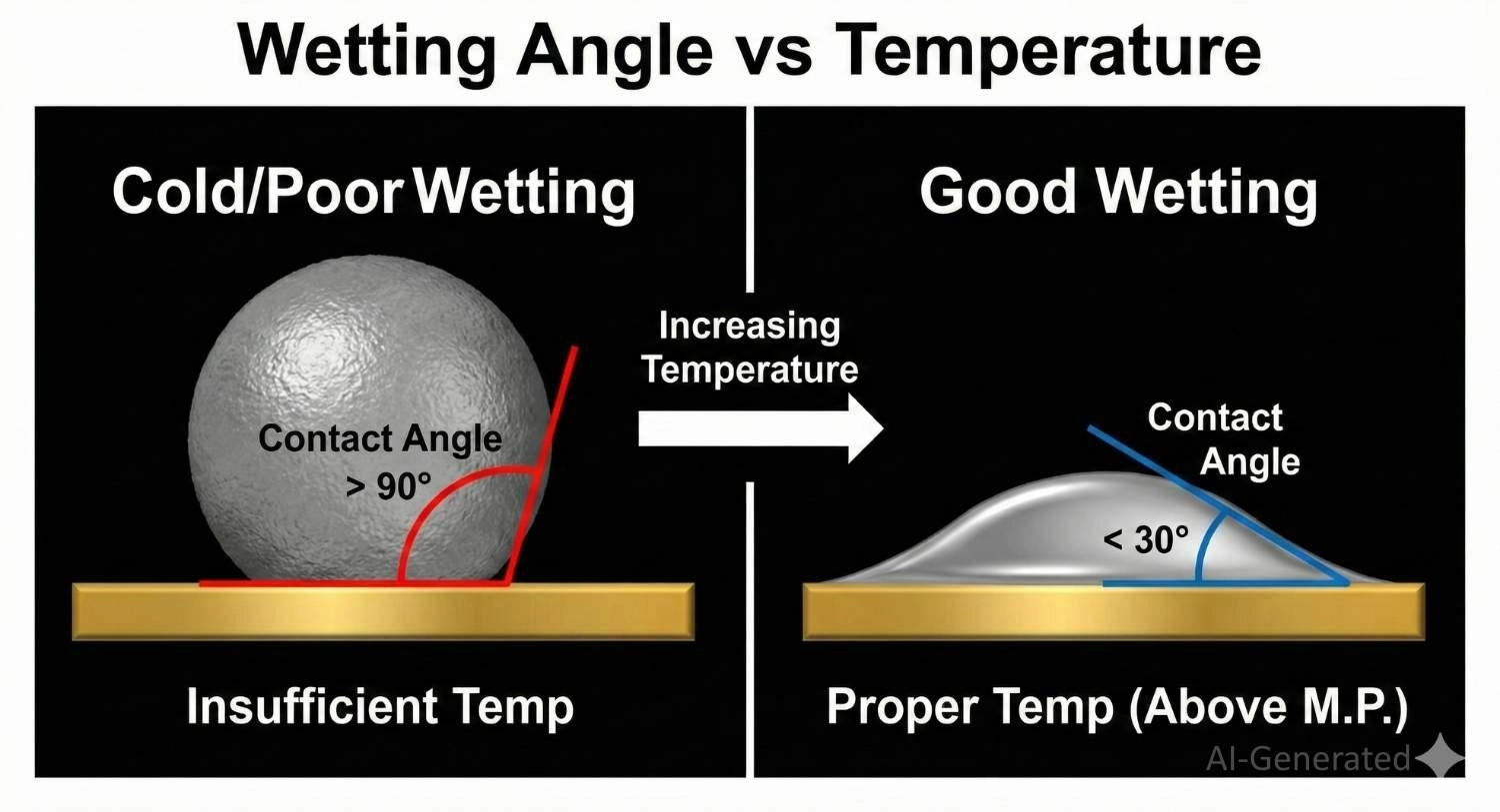
Showing solder wetting contact angles; less than 90 degrees indicates good bonding, while greater than 90 degrees indicates a cold solder joint.
What Does a Cold Solder Joint Look Like?
Identifying these defects relies heavily on visual analysis. To catch them before they leave the factory, you must know exactly what a cold solder joint looks like under magnification.
● Texture: A good joint is smooth and shiny (especially with SnPb solder). A cold joint often appears dull, grainy, rough, or crystalline. Note: Lead-free solders (SAC305) are naturally duller, so graininess alone is not always a defect, but a "dry" look is.
● Shape: Proper wetting creates a concave meniscus (fillet). A cold joint often looks convex, bulbous, or "balled up" because the solder's surface tension exceeded the adhesive force to the pad.
● Interface: You may see visible gaps or micro-cracks between the solder and the lead.
Cold Solder Joint vs Good Solder Joint
When evaluating a cold solder joint vs good solder joint, focus on the fillet shape.
● Good Solder Joint: Has a "volcano" shape with concave sides. The solder feathers out smoothly onto the pad.
● Cold Solder Joint: Looks like a "ball" sitting on the surface. The edges are abrupt, and the solder looks like it wants to pull away from the pad.
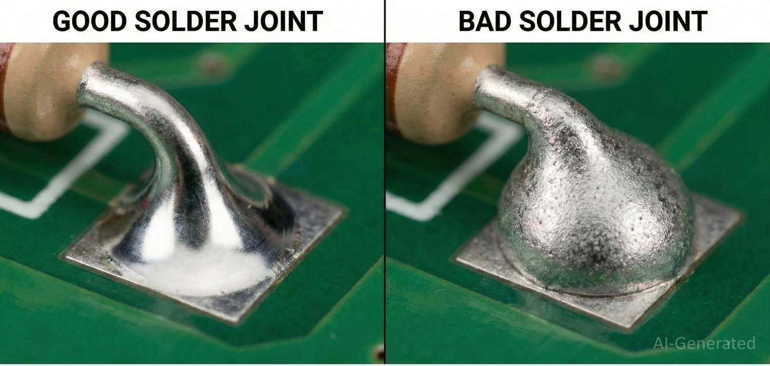
Macro comparison showing the difference between a cold solder joint vs good solder joint on a PCB.
Quick Diagnosis Checklist to Avoid Cold Joint
If you are inspecting a board under a microscope, use this checklist:
1. Is the solder dull or gray? → Likely insufficient heat (Cold Joint).
2. Is the surface grainy/rough? → Likely moved during cooling (Disturbed Joint).
3. Does the solder look like a ball sitting on the pad? → Poor wetting (Cold Joint).
4. Does the joint crack when poked with tweezers? → Mechanical failure.
Why Cold Solder Joints Are Dangerous?
Cold joints are insidious because they often pass simple continuity tests. However, they introduce several failure modes:
● Intermittent Electrical Connections: As the PCB heats up during operation, thermal expansion causes the board to flex, momentarily separating the weak bond.
● High Contact Resistance: The poor connection creates resistance, which generates localized heat (I²R losses), potentially burning the trace or damaging sensitive components.
● Vibration Vulnerability: In automotive or aerospace applications, the brittle nature of a cold joint means standard vibrations can cause a total fatigue fracture.
What Causes a Cold Solder Joint?
Understanding what causes a cold solder joint is the first step toward prevention. It is rarely just "one thing," but rather a combination of process variables that prevent proper wetting.
1. Insufficient Soldering Temperature
If the soldering iron or reflow oven does not reach the alloy's peak reflow temperature (typically ~245°C for lead-free), the solder remains in a semi-solid "pasty" state. It cannot wet the pad.
2. Improper Heating Time (Reflow Profile)
Even if the peak temp is reached, if the Time Above Liquidus (TAL) is too short, the flux doesn't have time to clean the oxides, and the IMC layer cannot form.
3. Thermal Mass Mismatch
Soldering a small component pin connected to a large ground plane without "Thermal Relief" pads causes the ground plane to act as a heat sink. It sucks heat away from the joint faster than the iron can supply it.
4. Movement During Solidification (Disturbed Joint)
If the component moves while the solder is cooling (transitioning from liquid to solid), the crystal structure is disrupted, resulting in a frosty, grainy appearance and high brittleness.
| Defect Type | Primary Cause | Visual Indicator |
|---|---|---|
| Cold Joint | Insufficient Heat / Poor Wetting | Bulbous shape, non-wetting to the pad. |
| Disturbed Joint | Movement during cooling | Frosty, wrinkled surface. |
| Dry Joint | Insufficient Flux | Irregular, spiky, or jagged shape. |
How to Identify a Cold Solder Joint
Professional assembly houses like JLCPCB use automated equipment, but manual identification is also possible.
1. Visual Inspection (Manual Check)
For prototypes or small batches, technicians use microscopes or magnifying lamps (Mantis viewers) to inspect joints. They look for the visual signs mentioned earlier, such as dullness, convex shapes, or micro-cracks. While flexible, this method is prone to operator fatigue.
2. Automated Optical Inspection (AOI)
AOI systems analyze solder joint shape, texture, and light reflection patterns. Cold solder joints often exhibit abnormal surface roughness or poor wetting, which can be flagged as defects. This is the standard for high-volume production.
However, AOI detects visual anomalies rather than electrical integrity.
3. Electrical Testing
Using a multimeter, set it to resistance mode (Ohms). A good joint should read near-zero resistance (excluding the component/trace resistance). If the reading fluctuates when you gently press or wiggle the component, you have found a cold joint.
4. X-Ray Inspection (AXI)
For Bottom Termination Components (BTCs) like BGAs or QFNs, visual inspection is impossible. X-Ray inspection is required to see "through" the chip. A cold joint under a BGA often appears as a lighter, less dense circle compared to properly reflowed balls or shows an irregular shape.
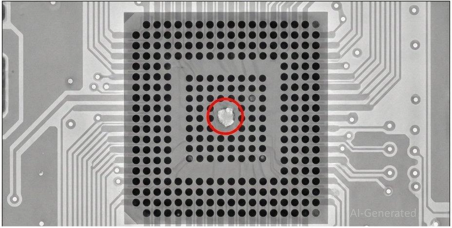
X-ray inspection revealing a cold solder joint void under a BGA component.
How to Fix a Cold Solder Joint
If you discover a defect, knowing how to fix a cold solder joint properly can save the board from the scrap bin.
Caution: Simply reheating the joint often fails because the original flux is burned off.
The Cold Solder Joint Rework Process:
1. Apply Flux: Add fresh flux to the joint. This is crucial to remove the oxides that formed during the failed attempt.
2. Reflow: Heat the joint with a soldering iron until the solder flows completely. You should see the "ball" collapse into a nice fillet.
3. Remove and Replace (If needed): If the solder looks heavily oxidized (gray/crusty), use a solder sucker or wick to remove the old solder entirely and re-solder with fresh wire.
For complex components, utilizing a Hot Air Rework Station is preferred over a soldering iron to ensure even heating.
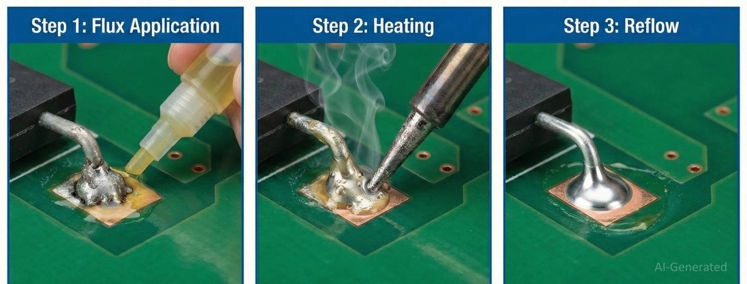
Step-by-step diagram of how to fix a cold solder joint using flux and a soldering iron.
When Rework Is Not Recommended:
Sometimes, attempting to fix a cold joint causes more harm than good. Avoid rework if:
● Pad Lifting: If the copper pad has started to peel off the FR4 substrate due to overheating, the board is structurally compromised.
● Heat-Sensitive Components: Devices like crystals, LEDs, or plastic connectors may melt or lose calibration with repeated heating cycles.
● Severe Oxidation: If the pad is black or heavily corroded, solder will likely never wet properly, even with flux. The PCB is likely scrap.
● Impossible Access: In densely packed High-Density Interconnect (HDI) boards, if the iron tip cannot reach the joint without desoldering neighbors, rework is too risky.
How to Prevent Cold Solder Joints in PCB Assembly
Prevention is always cheaper than rework. JLCPCB’s SMT (Surface Mount Technology) service implements strict controls to ensure how to prevent cold solder joints is baked into the process.
1. Optimizing Reflow Profiles
The temperature curve of the reflow oven is critical.
● Soak Zone: Allows the flux to activate and equalize the temperature across the board.
● Reflow Zone: Ensures the solder stays above liquidus (TAL) usually for 45-90 seconds to ensure total wetting.
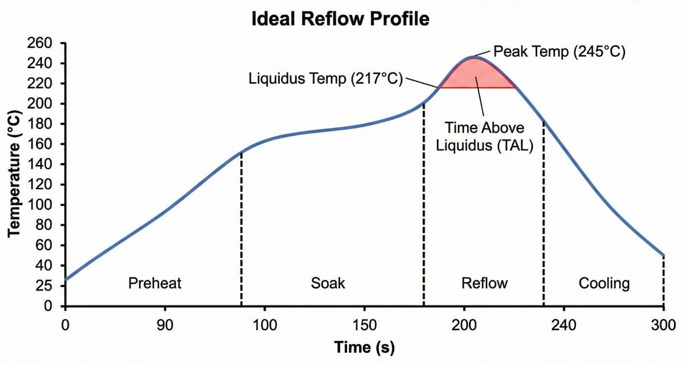
SMT reflow profile chart showing the time above liquidus to prevent cold solder joints.
2. Design for Manufacturability (DFM)
Designers must account for thermal distribution. Avoid connecting pads directly to large copper pours. Use thermal relief patterns (spokes) to thermally isolate the pad, allowing it to heat up quickly during reflow.
Learn More: Design for Manufacturing (DFM): A Comprehensive Guide for Optimizing Production
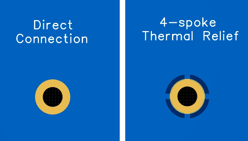
PCB layout comparison showing thermal relief spokes versus direct connection to ground plane.
3. Proper Flux Selection
Using an expired or weak flux prevents oxide removal. Ensure the flux activity level matches the oxidation level of the components (e.g., using Rosin Activated (RA) flux for older, oxidized leads).
4. Component Storage
Moisture and oxidation on the component leads are major causes of non-wetting. Using fresh components from reliable suppliers ensures the leads are pristine and ready to solder.
Cold Solder Joint vs Other Solder Defects
It is easy to confuse cold joints with other issues. Here is a quick breakdown:
● Cold Solder Joint vs Dry Solder Joint: A cold joint usually has enough solder but insufficient heat. A dry joint (often used interchangeably) specifically refers to a joint where the solder has "dried out," or flux was insufficient, leading to open circuits.
● Cold Solder Joint vs Insufficient Solder: Insufficient solder means the fillet is concave but too small (starved). A cold joint typically has enough solder volume, but the shape is wrong (convex).
● Cold Solder Joint vs Cracked Solder Joint: A cracked joint may have been soldered perfectly originally, but failed due to mechanical stress or thermal cycling later.
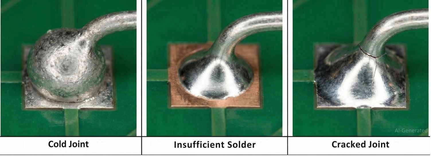
Comparison of cold solder joint vs insufficient solder vs cracked solder joint.
Industry Standards Related to Cold Solder Joints
To ensure reliability, engineers follow strict standards:
● IPC-A-610: The primary standard for electronic assembly acceptance. It defines a cold solder joint as a defect for all classes (Class 1, 2, and 3).
● J-STD-001: Specifies the material and process requirements to produce high-quality soldered interconnections.
For critical industries (Medical, Automotive), strictly adhering to Class 3 requirements is mandatory, which allows for zero visible cold joint anomalies.
Conclusion
A cold solder joint is more than a cosmetic blemish; it is a reliability time bomb. Whether caused by insufficient heat, contaminated surfaces, or poor design, the result is the same: device failure.
By understanding the physics of wetting, utilizing proper reflow profiles, and adhering to DFM guidelines, you can drastically reduce these defects. However, the best prevention is partnering with a manufacturer that understands these nuances. At JLCPCB, our advanced SMT lines utilize AOI, X-Ray, and precise thermal profiling to ensure every joint meets rigorous industrial standards.
FAQs about Cold Solder Joint
Q1. Why do cold solder joints frequently occur on ground connections?
Ground pins are connected to large copper planes that act as massive heat sinks. Without "thermal relief" patterns in the design, the copper plane sucks heat away from the soldering iron faster than it can be applied, preventing the joint from reaching the liquidus temperature needed for wetting.
Q2. Can I simply reheat a cold solder joint to fix it?
No. Simply reheating is rarely effective because the original flux has already burned off. To fix it properly, you must apply fresh flux to break the oxidation layer. If the joint is heavily oxidized, it is best to remove the old solder completely and re-solder.
Q3. Does mixing leaded and lead-free solder cause cold joints?
Yes. Mixing alloys (like SnPb and SAC305) can create a "segregated" joint because they have different melting points (183°C vs 217°C). This can result in a grainy, weak structure that mimics a cold solder joint and is prone to cracking.
Q4. What is the typical resistance of a cold solder joint?
While a good solder joint has negligible resistance (<0.1Ω), a cold joint can vary wildly. It might read 10Ω, 100Ω, or even show an open circuit (OL). The most dangerous characteristic is that the resistance often fluctuates with temperature changes.
Q5. Does the PCB surface finish affect cold joint formation?
Yes. Certain finishes like OSP (Organic Solderability Preservative) degrade faster if stored improperly, leading to oxidation that prevents wetting. ENIG (Electroless Nickel Immersion Gold) is generally more resistant to oxidation and promotes better wetting, reducing the risk of cold joints during reflow.
Popular Articles
• Common PCB Assembly Methods and Soldering Techniques Explained
• What Is BGA Void? Causes, IPC Limits, and Solutions
• SMD Soldering Tools You Need: Complete Guide from Beginner to Pro
• Reflow Soldering: Everything You Need to Know
• SMT Assembly Process Explained and Equipment Used: A Step-by-Step Guide to PCBA Manufacturing
Keep Learning
12 Professional Soldering Tips and Tricks Every Beginner Should Know
Soldering is not merely "gluing" metal; it is a metallurgical process that creates an intermetallic compound (IMC). This molecular bond ensures the electrical and mechanical integrity of your device. A poor joint might pass a quick visual check but will inevitably fail under vibration or thermal stress, leading to "ghost" bugs and hardware failures. These soldering tips and tricks focus on practical, repeatable techniques used in professional electronics soldering—from correct heat transfer and flux u......
Solder Melting Point Guide: Chart, Alloy Types, and Reflow Considerations
In the precise world of electronics manufacturing, a difference of just a few degrees can mean the distinction between a perfect, reliable solder joint and a catastrophic "cold" joint failure. While many hobbyists view soldering simply as "melting metal to stick things together," professional PCB assembly requires a nuanced understanding of thermodynamics. The solder melting point is not simply a single value listed in a datasheet; it is a decisive limit that determines the choice of components, the s......
The Ultimate Guide to Solder Flux: Everything You Should Know Before Soldering PCB
Soldering is needed to make almost all electronic devices. Adding solder alone won't make a joint that is strong, clean, and sound from a metallurgical point of view. Solder flux is a very important part of the process that comes in here. If you want to do your job better and make it more reliable, you need to know a lot about soldering flux, whether you're an engineer, a professional technician, or just a hobbyist. This article goes into a lot of detail about solder flux, including what it is, how it......
Common PCB Assembly Methods and Soldering Techniques Explained
Whether you're designing your first prototype or scaling up to production, understanding PCB assembly methods and soldering techniques is crucial to achieving reliable, high-performance circuit boards. Modern PCBA primarily relies on Surface Mount Technology (SMT) and Through-Hole Technology (THT)—each offering unique advantages for component density, durability, and manufacturability. In this guide, we'll break down the major PCB assembly methods, key soldering techniques such as reflow and wave sold......
Flex PCB Assembly Guide: Process, Challenges, and Solutions
Flexible Printed Circuit Boards (Flex PCBs) are the foundational technology enabling the compact, innovative design of modern electronics. Because of their ability to bend and fold, they power devices from smart wearables to compact medical instruments where traditional rigid printed circuit boards (Rigid PCBs) can't be used. Achieving a functional electronic circuit from the raw plastic film demands special expertise, with flexible PCB assembly (FPCA) representing the crucial final step in this trans......
SMD Rework Guide: Tools, Temperatures, and Techniques That Prevent PCB Damage
From replacing a burned regulator to correcting wrong component values or removing solder bridges on fine-pitch ICs, SMD rework is an essential skill in electronics manufacturing and prototyping. It allows engineers to repair assembly defects, implement design changes, and recover valuable PCBs without the cost and delay of building new boards. In this guide, you will learn: What SMD rework is Common rework scenarios Tools and temperatures Safe removal and installation Package-specific techniques Real......