
Laser Cut Stencil for PCB Assembly: Materials, Machines, and Key Advantages
11 min
- What Is a Laser Cut Stencil in PCB Assembly?
- Materials and Equipment for Laser Cut Stencil
- Advantages and Sourcing of Laser Cut Stencil
- Conclusion
Modern surface mount assembly relies on precise solder paste transfer across dense PCB pad arrays. Inconsistent paste volume produces opens, solder bridges, and unstable joints during reflow. PCB stencils control paste deposition through apertures that match copper land patterns, ensuring accurate and repeatable printing.
Laser cut stencils achieve high dimensional accuracy with uniform aperture walls, which improve paste release for fine pitch components. These stencils handle prototype and production assemblies without sacrificing print quality. JLCPCB stencil services supply laser cut stencil products that integrate smoothly with automated SMT printers, delivering consistent solder paste deposition across complex PCB layouts.
What Is a Laser Cut Stencil in PCB Assembly?
Definition of a Laser Cut Stencil
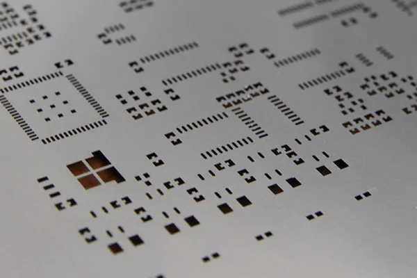
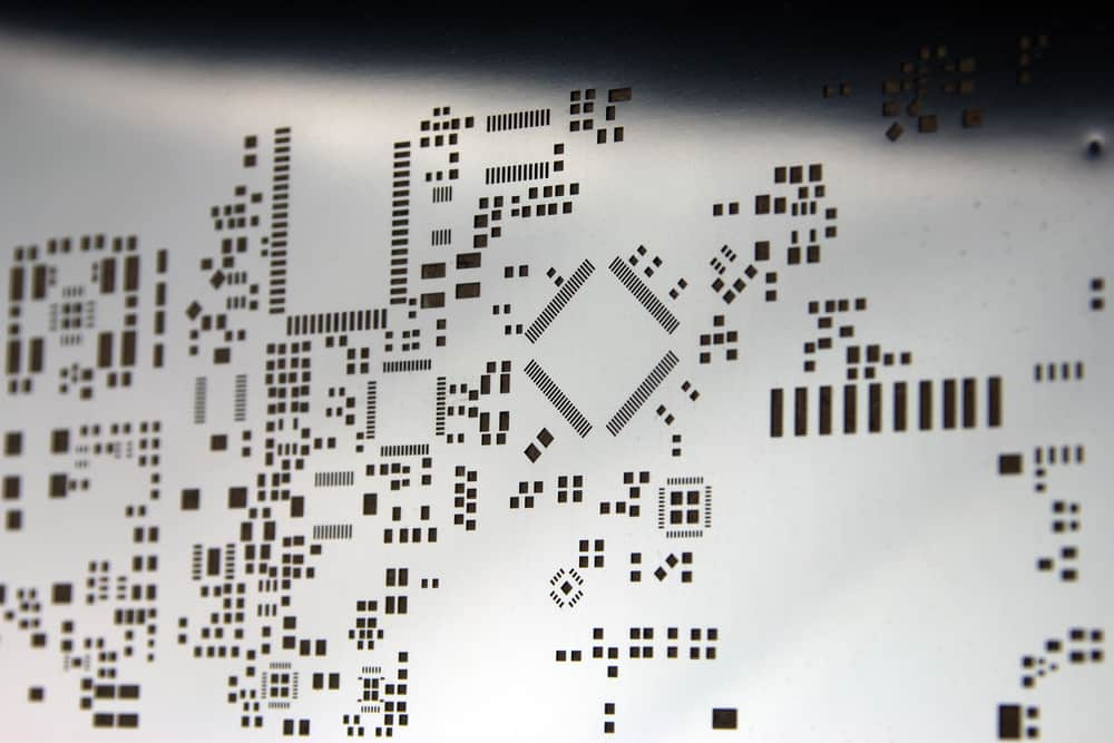
A laser cut stencil is a thin sheet of metal, usually stainless steel, patterned with precise apertures aligned to PCB solder pads. These apertures regulate the deposition of solder paste during surface mount technology assembly, controlling the exact volume applied to each pad. Laser cut stencils differ from chemically etched or mechanically punched stencils because they provide consistent aperture walls, uniform thickness, and sharp corners.
The stencil material for laser cutting, often stainless steel or nickel alloy, maintains flatness and resists bending under printer pressure. JLCPCB stencil services manufacture laser cut stencils with micron-level accuracy, allowing repeated use across multiple PCB runs without degradation.
Typical Applications in PCB Assembly
Laser cut stencils play a decisive role in PCB assembly, especially where solder paste accuracy affects electrical performance and joint reliability. Their precision and repeatability make them suitable for various applications, which includes:
1. BGA Placement: Laser cut stencils deposit solder paste onto each ball pad with micron-level accuracy, preventing bridging and void formation. They maintain consistent paste volume across high-density arrays.
2. QFN Components: These stencils provide precise paste coverage for quad flat no-lead ICs, ensuring solder joints form evenly on pads beneath the package body.
3. Microcontrollers: Fine-pitch pins on microcontrollers require uniform paste deposition. Laser cut stencils guarantee alignment and volume control for reliable signal connections.
4. LED Arrays: Arrays of surface mount LEDs demand even paste spread to prevent misalignment and inconsistent brightness. Laser cut stencils produce repeatable deposition across large arrays.
5. High-Density Connectors: Stencils manage solder deposition for connectors with minimal spacing between pins, reducing bridging and tombstoning risks.
6. Prototype PCB Boards: Stencils deliver accurate printing for prototypes, where pad geometries vary, and tolerances are tight, reducing the need for post-reflow correction.
7. Medium-Volume Production Runs: Laser cut stencils maintain consistent paste deposition over multiple boards, ensuring uniform joint formation and reducing defects.
8. Industrial Sensor Modules: Precision stencils deposit paste for sensitive sensor boards, maintaining signal integrity and mechanical stability under operational stress.
9. High-Performance Computing and Communication Boards: Dense layouts with fine-pitch ICs, memory modules, and connectors rely on laser cut stencils to achieve reliable solder joints under thermal and electrical loads.
JLCPCB laser cut stencils accommodate both prototype and production boards. Their precise aperture alignment ensures consistent paste deposition for automated SMT printers. These stencils meet requirements across industrial, consumer, and high-performance electronic applications, improving PCB assembly reliability and repeatability.
Why Laser Cutting Is Preferred for PCB Stencils?
Laser cutting produces apertures with precise edges, uniform wall thickness, and exact dimensions, which directly control solder paste volume and print quality. The accuracy of aperture walls determines the amount of paste deposited on each pad, reducing the risk of solder bridging or insufficient solder. Mechanical punching creates burrs at aperture edges, while chemical etching generates tapered or uneven walls, both of which compromise fine pitch assembly and print repeatability.
Laser stencil cutting machines allow precise control over aperture geometry, wall thickness, corner radii, and metal grain orientation. Controlling these factors improves repeatable printing, which is essential for fine pitch components below 0.4 millimeters. Uniform aperture walls allow solder paste to release cleanly onto PCB pads, ensuring consistent joint volume and alignment across the board.
Stencil flatness and rigidity, achieved through proper laser cutting and high-quality metal selection, prevent bowing or warping during printing. High flatness ensures uniform contact between stencil and PCB, reducing defects such as incomplete paste transfer and void formation. Laser cut stencils maintain these properties over repeated use, supporting both prototype and medium-volume production runs.
JLCPCB laser cut stencils deliver micron-level aperture accuracy, high flatness, and long operational lifespan. These stencils reduce bridging, tombstoning, and other solder defects while improving assembly yield. Manufacturers prefer laser cut stencils for critical SMT applications where repeated, precise printing determines board quality, fine pitch compatibility, and electrical reliability. Laser cut stencils outperform chemical and mechanical alternatives in repeatability, durability, and print consistency.
Materials and Equipment for Laser Cut Stencil
Stencil Material for Laser Cutting
The selection of stencil material for laser cutting directly affects solder paste deposition, aperture precision, and SMT assembly reliability. Material properties such as hardness, thermal stability, and corrosion resistance determine how well a stencil maintains flatness and aperture definition under repeated use.
Common materials for laser cut stencils include:
1. Stainless Steel: The most widely used material, stainless steel provides high hardness, excellent corrosion resistance, and thermal stability during reflow and cleaning cycles. It maintains aperture shape without warping, making it suitable for fine pitch ICs and high-density PCB layouts.
2. Nickel Alloys: Nickel-based alloys offer long stencil lifespan and superior rigidity for repeated SMT runs. They resist bending under printer pressure and tolerate cleaning with solvents, ensuring consistent aperture walls.
3. Phosphor Bronze (Occasionally): Some specialty applications use phosphor bronze for flexible stencils where precise spring-back and controlled elasticity are required, typically in custom prototype scenarios.
4. Copper (Rare Cases): Copper stencils appear in experimental or high-conductivity applications, but their softness requires careful handling and additional coating to prevent aperture deformation.
Material choice influences aperture wall smoothness, flatness, and print repeatability. Stainless steel and nickel alloys resist bowing and deformation during cleaning and printing, which ensures uniform solder paste deposition for fine pitch components below 0.4 millimeters.
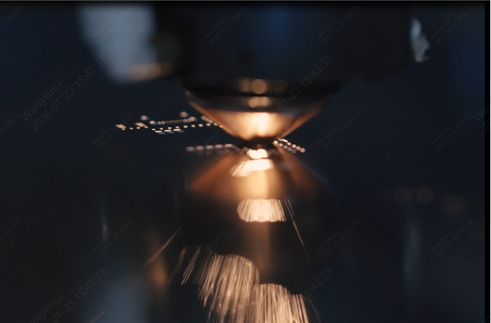
Laser Stencil Cutting Machine Overview
Laser stencil cutting machines use high-precision fiber or CO₂ lasers to create apertures in metal sheets according to CAD-defined PCB patterns. These lasers deliver focused energy that vaporizes the metal without deforming the surrounding areas. The result is sharp aperture edges and uniform wall thickness, which directly influence solder paste volume and release during SMT printing.
Modern machines control key parameters, which include:
● Beam intensity
● Pulse duration
● Scanning speed
● Focal depth
Adjusting these factors ensures apertures meet micron-level tolerances, which is essential for fine-pitch components below 0.4 millimeters. Consistent laser operation prevents defects like tapered walls, burrs, or incomplete cuts that compromise solder paste transfer.
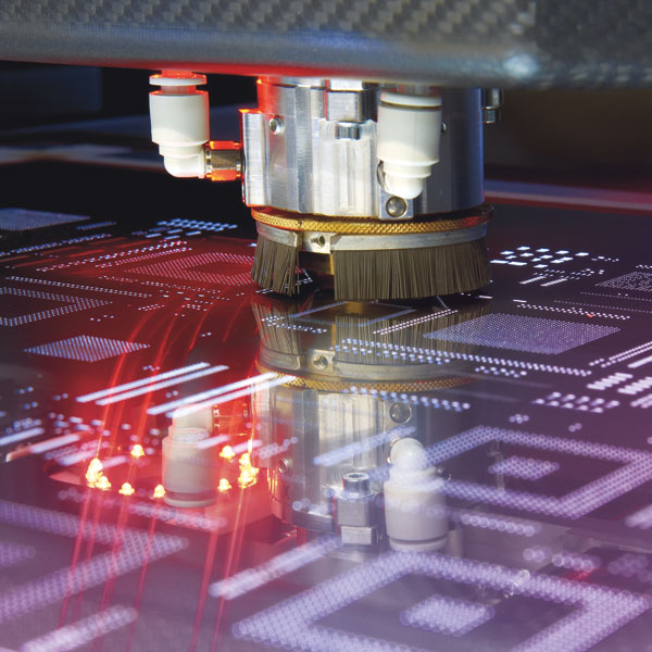
Automated positioning systems secure the metal stencil during cutting and maintain alignment with CAD patterns. Vision inspection systems verify aperture dimensions in real time, detecting deviations before the stencil leaves the production line. These features reduce errors and improve repeatability across both prototype and medium-volume production boards.
Laser stencil cutting machines handle various metal thicknesses, typically ranging from 75 to 150 micrometers. They accommodate different materials such as stainless steel and nickel alloys, preserving flatness and wall rigidity during cutting.
How Equipment and Material Affect Stencil Quality
Stencil quality depends on the metal’s physical properties and the precision of the laser cutting machine. Rigid, flat metal resists bowing during printing, ensuring uniform contact between stencil and PCB. Material hardness and thermal stability influence aperture retention during repeated printing and cleaning cycles.
Uniform aperture walls control solder paste volume and release, reducing defects such as bridging or insufficient solder. Smooth, straight walls maintain consistent deposition across all pads. Laser parameters including pulse duration, power, and scan speed determine edge sharpness and wall uniformity.
Fine pitch components below 0.4 millimeters require strict control of material thickness and laser accuracy. Stencil flatness and precise beam focus prevent misalignment, solder bridging, or tombstoning. Both material quality and laser precision directly influence repeatable printing and assembly reliability.
Advantages and Sourcing of Laser Cut Stencil
Advantages of Laser Cut Stencils
Laser cut stencils provide precise control over solder paste deposition, aperture geometry, and assembly reliability. Their accuracy and repeatability make them essential for fine pitch and high-density PCB assembly. The advantages of laser cut stencils are listed below:
1. High Dimensional Accuracy: Laser cut stencils maintain exact aperture dimensions according to CAD or Gerber files. Accurate apertures control solder paste volume precisely, ensuring consistent electrical and mechanical connections.
2. Uniform Aperture Walls: Smooth, straight walls regulate paste release, reducing solder bridging, tombstoning, and void formation during reflow. Consistent wall geometry improves paste transfer for both small and large components.
3. Flatness Retention: High-quality metal sheets resist bending and maintain flat contact with the PCB. This prevents uneven paste deposition and reduces defects during repeated printing and cleaning cycles.
4. Fine Pitch Component Compatibility: Laser cutting produces apertures for components with pitch below 0.4 millimeters, such as BGAs, QFNs, and fine-pitch ICs, which are challenging for mechanical or chemical etching methods.
5. Burr-Free Aperture Edges: Clean, sharp edges minimize paste smearing and improve transfer efficiency, which is critical for high-density and complex PCB layouts. Burr-free apertures also reduce the need for post-print inspection or rework.
6. Long Operational Lifespan: Laser cut stencils maintain aperture accuracy and flatness over multiple prints, supporting both prototype testing and medium-volume production runs. Durable stencils reduce replacement frequency and production downtime.
7. Reduced Defect Rates: Combining precise apertures, uniform walls, and flat material significantly decreases soldering defects, improving SMT assembly yield.
Laser cut stencils integrate high-precision manufacturing with quality metal selection to deliver repeatable solder paste deposition. The advantages of laser cut stencils enhance assembly reliability, reduce defects, and support both prototype and production board requirements.
Production vs Prototype Use Cases
Laser cut stencils suit both prototype and production SMT assembly, with different requirements for stencil thickness, material, and laser parameters. Prototypes require precise paste deposition on experimental PCB layouts, while production boards demand repeatable printing and high reliability across multiple units. The table below summarizes key differences:
| Aspect | Prototype Boards | Production Boards |
| Purpose | Test experimental PCB layouts and new designs | High-volume or medium-volume assembly with consistent quality |
| Stencil Thickness | 75–100 micrometers | 100–150 micrometers |
| Material | Stainless steel or nickel alloy | Stainless steel or nickel alloy, optimized for durability |
| Paste Deposition | Accurate deposition on varying pad geometries | Repeatable deposition across multiple boards |
| Component Type | Fine pitch ICs, small connectors, and LEDs | Fine pitch ICs, BGAs, high-density connectors |
| Printing Repeatability | Moderate, sufficient for prototype testing | High, required for consistent production yield |
| Defect Risk | Lower volume minimizes the impact of minor errors | A low defect rate is essential for production efficiency |
| Lifecycle | Short-term use, mainly testing | Medium-term use, multiple print cycles per stencil |
Laser cut stencils for prototypes provide flexibility in design testing, while production stencils focus on repeatable performance, consistent paste transfer, and reduced defect rates. Material selection and laser cutting parameters are essential in both cases to ensure high-quality solder joints across different board types.
Finding Laser Cut Stencils Near Me or Online
Laser cut stencils near me are available from specialized SMT suppliers who produce stencils based on CAD or Gerber files. Suppliers offer options for prototype and production boards, allowing selection of material, thickness, and aperture tolerance. Accurate stencils ensure consistent solder paste deposition for fine pitch and high-density layouts.
Many suppliers, including JLCPCB, provide online ordering for laser cut stencils. Engineers can upload Gerber files and select stencil specifications, producing stencils suitable for prototypes and medium-volume SMT production with precise aperture geometry and high flatness.
Local electronics manufacturers may offer stencil fabrication for immediate needs, reducing lead times for prototypes or urgent runs. Proper sourcing ensures aperture consistency, long-term durability, and reliable solder paste deposition, improving PCB assembly yield.
Conclusion
Laser cut stencils are necessary for reliable PCB assembly. They deliver precise solder paste deposition, uniform aperture geometry, and consistent print results across all board types.
High-quality stencil material, such as stainless steel or nickel alloys, combined with precise laser cutting, ensures flatness, durability, and compatibility with fine pitch components. Correct equipment and material selection reduces defects and improves assembly reliability.
Verified suppliers provide stencils that maintain aperture accuracy and long-term usability. JLCPCB offers online ordering with custom specifications, enabling engineers and manufacturers to produce prototype and production boards with consistent solder paste deposition and improved SMT assembly yield.

Keep Learning
SMT Stencil Cleaning Guide: Process, Frequency, and Tips
Key Takeaways about SMT Stencil Cleaning SMT stencil cleaning removes solder paste residue from aperture walls and the stencil underside, keeping paste transfer efficiency between 80% and 100%. Industry analysis attributes over 60% of SMT defects to the paste-print step — most of which trace back to a stencil cleaning lapse. Two stages matter: under-screen cleaning (between cycles, typically every 5–10 prints) and off-line cleaning (after production completes). IPA handles standard flux residue; dedic......
Top 5 Circuit Board Stencil Mistakes & How to Fix Them for Higher SMT Yield
Usually, the circuit board stencil is responsible for roughly 60% to 70% of all SMT defects. That number surprises people. It shouldn't. The stencil controls paste volume, deposit geometry, and positional accuracy all at once. When it gets wrong, everything downstream pays for it. The shift in thinking that separates good engineers from great ones is simple: stop seeing the PCB stencil as a metal sheet with holes in it. It is a precision fluid delivery system. Every aperture wall, every micron of foil......
How to Apply SMD Glue Using SMT Stencils (Design, Thickness & Troubleshooting Guide)
The reality of modern PCB assembly is that "mixed-technology" is still very much the norm. When a board hits the wave soldering machine, bottom-side SMD components face a high-velocity river of molten metal. Without a solid mechanical bond, they’ll simply wash away into the solder pot. That’s where the precision application of SMD glue becomes the difference between a successful run and a bin full of scrap. Quick Answer: How to Apply SMD Glue in SMT If you need to configure your SMT stencil for adhesi......
The Essential Guide to SMT Stencils in PCB Assembly
Introduction In the dynamic world of electronics manufacturing, Surface Mount Technology (SMT) plays a crucial role in achieving efficiency and precision in printed circuit board (PCB) assembly. Central to the SMT process is the SMT stencil, an indispensable tool for the accurate application of solder paste. This ensures solid electrical connections between components and PCBs. This guide delves into the specifics of SMT stencils, examining their types, materials, manufacturing methods, advantages, ch......
Nano-Coatings in PCB Manufacturing: How They Outperform Traditional Stencils
Nano coating is a thin hydrophobic (water repellent) and oleophobic (oil repellent) treatment used on the undersides and edges of solder paste stencils. With this the surface becomes non-stick which reduces the number of cleaning cycles required for the solder paste printing process. Upon application, the less than 5 nanometer coating bonds with the stencil foil at the microscopic level, which does not change the size and shape of the stencil. Nano coating is an industry proven process which shows imm......
How to Choose an SMT Stencil
What is an SMT stencil? SMT Stencil is a thin metal sheet used in the soldering process for SMT (Surface Mount Technology) and it plays an essential role in the SMT soldering process. Smt Stencil allows the direct placement of solder paste onto the SMD pads of PCB, which can help prevent errors and defects during the reflow soldering process. This results in a precise amount of tin coverage once the work is completed. Types of SMT Stencils Depending on the application of solder paste, there are three ......