
3D Printed PCB Explained: Technology, Materials, Pros, Cons, and Applications
21 min
- What Is a 3D Printed PCB?
- How 3D Printed PCBs Differ from Traditional PCBs
- 3D Printed PCB Manufacturing Methods
- Materials Used in 3D Printed PCBs
- 3D Printed PCB Design and Prototyping Workflow
- Pros and Cons of 3D Printed PCBs
- 3D Printed PCB Applications and Use Cases
- JLCPCB's Role in Practical 3D Printed PCB Prototyping
- Conclusion
- FAQ about 3D Printed PCBs
3D printed PCBs are redefining how electronic circuits can be designed, prototyped, and integrated into complex structures. Unlike traditional FR-4 boards, this additive manufacturing approach enables conformal geometries, structural electronics, and rapid iteration without tooling or chemical etching.
This article explains what 3D printed PCBs are, how they work, their key advantages and limitations, and how they compare to conventional PCBs—helping engineers and product designers understand when this technology makes sense and when traditional PCB fabrication remains the better choice.
What Is a 3D Printed PCB?
A 3D printed PCB is a circuit board created using additive manufacturing techniques, rather than traditional subtractive methods like etching copper from a flat laminate. Instead of starting with a solid board and removing material, 3D printing builds the PCB layer by layer, combining insulating substrates and conductive traces directly in the desired geometry.
Unlike conventional flat PCBs, 3D printed boards can take non-planar, curved, or custom-shaped forms, allowing electronics to integrate seamlessly into enclosures, wearable devices, or structural components. This approach also enables rapid prototyping, as digital designs can be quickly turned into functional boards without the long lead times of traditional fabrication.
In practice today, fully 3D printed PCBs are mostly used for research and prototypes. Most applications adopt a hybrid approach, where traditional PCBs provide reliable electrical performance, while 3D printed parts add mechanical structures, flexible substrates, or custom housings.
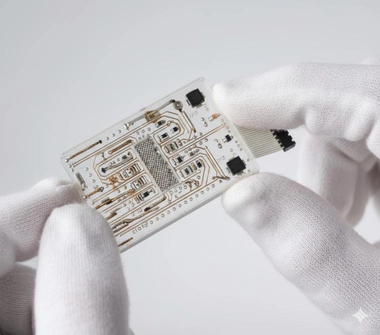
A 3D printed PCB with assembled SMD components
How 3D Printed PCBs Differ from Traditional PCBs
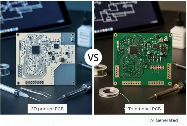
In traditional PCB manufacturing, including rigid, rigid-flex, and multilayer designs, circuits are fabricated using subtractive processes such as copper etching and lamination on flat substrates like FR-4.
This approach is highly mature and efficient for planar, two-dimensional layouts, especially in high-volume production. However, it introduces fundamental limitations when electronic designs must conform to complex three-dimensional requirements.
3D Printed PCBs vs Traditional PCBs: Key differences
● Manufacturing Method: Traditional PCBs rely on subtractive fabrication, while 3D printed PCBs use additive manufacturing to build both structure and circuitry layer by layer.
● Geometric Freedom: Conventional PCBs are inherently planar, whereas 3D printed PCBs enable conformal geometries, allowing circuits to wrap around curved or irregular surfaces.
● Structural Integration: In traditional designs, the PCB and mechanical enclosure are separate parts. With 3D printed PCBs, electronic traces can be directly integrated into the structural body itself, enabling structural electronics.
● Assembly Complexity: Flat PCBs often require connectors, cables, and mounting hardware to fit into three-dimensional housings. 3D printed PCBs can reduce or eliminate these components by embedding conductive paths directly within the structure.
● Electrical Performance Comparison: Traditional PCBs use copper traces with low resistivity, supporting high-current and high-frequency circuits. 3D printed PCBs have higher resistivity and variable properties, making them suitable mainly for prototyping and low- to medium-power applications.
● Mechanical and Thermal Comparison: FR-4 boards offer high strength and thermal stability. 3D printed PCBs provide flexible geometries but lower mechanical and thermal limits, fitting lightweight, low-stress applications like wearables or custom enclosures.
● Manufacturing Cost and Scalability: Traditional PCBs are optimized for high-volume, low-cost production. 3D printed PCBs are best for rapid, low-volume prototyping, with higher material and time costs limiting mass production.
These differences explain why 3D printed PCBs are primarily adopted for prototyping, custom geometries, and low-volume applications, rather than as a direct replacement for conventional FR-4-based PCBs in mass production.
3D Printed PCB Manufacturing Methods
Creating a 3D printed PCB involves precise additive manufacturing of two very different materials: the insulating substrate and the conductive traces. Unlike traditional subtractive PCB methods, additive approaches allow for more complex geometries and integrated structures. There are three major methods used today:
Method 1: Direct Printing of Conductive Traces (Ink-Based Methods)
Note: This approach is primarily for prototyping and specialized applications, rather than large-scale commercial production.
This is the most conceptually advanced method, where the circuitry is built using specialized conductive materials precisely deposited onto the substrate.
● High-Resolution Ink Systems: Conductive and dielectric inks are printed layer by layer to form the PCB.
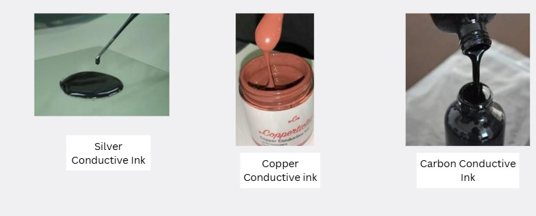
● Conductive Inks: Usually, these are non-Newtonian fluids—special inks that consist of fine nanoparticle suspensions of materials like silver, copper, or graphite. Silver is the most widely used material because of its excellent electrical conductivity and relative stability.
● Process Capability: These systems can print the entire board from scratch, producing complex, multilayered, and double-sided PCBs with vertical interconnects (vias). Advanced applications, such as the example by Hensoldt, demonstrate the printing of multi-layer (e.g., 10-layer) boards that integrate high-performance structures, proving their potential for complex sensor applications.
● Trace Creation: Processes like Aerosol Jet Printing utilize an aerosol-laden stream to produce fine traces (often down to 10 μm) while Inkjet Printing accurately releases droplets. They are also capable of printing special components directly, such as coils, resistors, or even embedded LEDs.
Method 2: FDM-Based 3D Printed PCBs Using Conductive Filaments
Fused Deposition Modeling (FDM) allows low-cost prototyping using thermoplastic filaments mixed with conductive particles (e.g., graphene or carbon black).
● Materials: Conventional FDM printers extrude filaments (like PLA, ABS, TPU) that are mixed with conductive particles like graphene or carbon black.
● Trade-offs: Despite being highly economical and very much compatible with nearly all FDM printers, this technique leads to the production of circuitry that is inherently bulkier and less electrically efficient due to higher resistivity. Therefore, it is appropriate for rapid, early-stage prototyping and structural mockups but is not applicable for high-frequency or high-current commercial operations.
The higher resistivity and limited trace resolution make FDM-based PCBs unsuitable for high-speed or high-current circuits.
Method 3: Substrate-First 3D Printed PCBs with Hollow Channels
The method fundamentally distinguishes the two main aspects of printing, i.e., the structural part and the conducting part, so that the circuit’s physical channel can be made using standard 3D printers.
● Process: In the beginning, the process is to print a non-conductive solid block (the "case") using common FDM materials, like ABS or PLA. Within this printed block, the channels or trenches that define the path of the future conductive traces are very accurately designed.
● Conductive Filling: After the structural printing is complete, a post-processing operation fills the hollow spaces with a conductor substance, such as electric paint, conductive epoxy, or via electroless plating (as is often used with Selective Laser Sintering, or SLS, printed parts).
● Advantages: This method offers higher conductivity compared to many directly printed conductive filaments and provides access to almost any sufficiently precise 3D printer, hence a very affordable option for circuit carrier manufacturing. This approach can reduce post-print soldering steps for certain low-power or embedded applications, though some electrical connections may still require manual finishing.
This approach is widely used for custom enclosures, low-power embedded circuits, and hybrid prototypes.
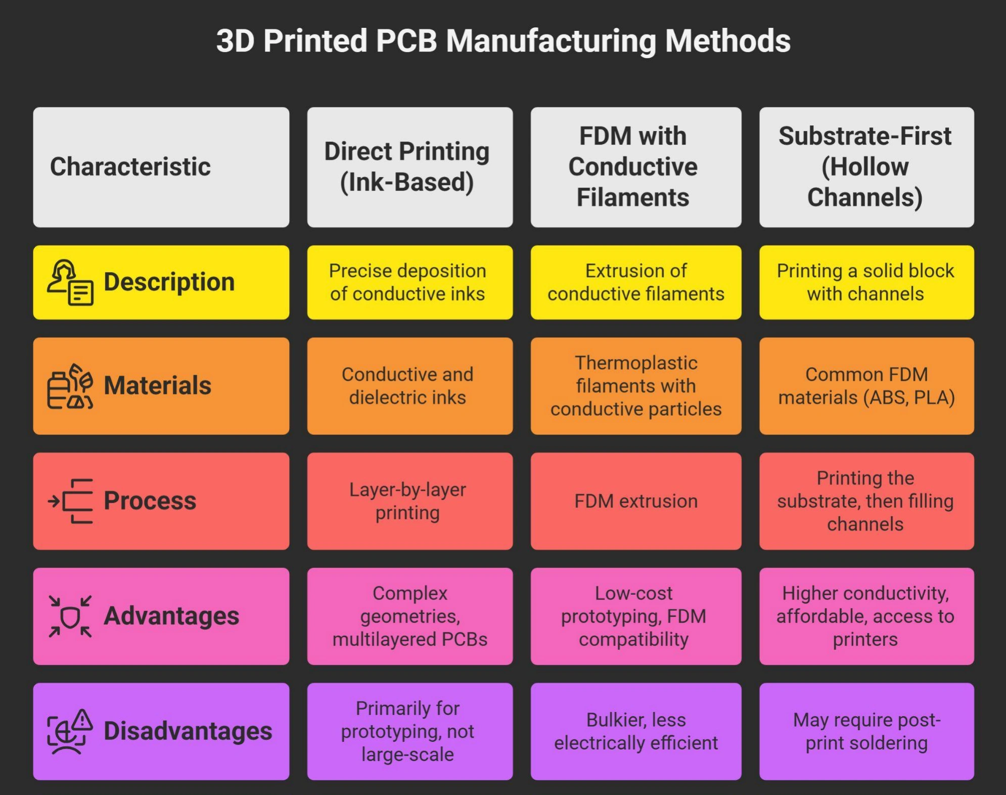
3D printed PCB manufacturing methods
Materials Used in 3D Printed PCBs
The choice of materials is a key factor in 3D printed PCB design, affecting structural integrity, electrical performance, and thermal reliability.
Insulating Materials for 3D Printed PCB Substrates
Common insulating substrates include PLA, ABS, and specialized photopolymers. These materials provide the physical structure for the circuit but come with thermal and mechanical limitations:
● PLA softens around 60 °C, limiting high-temperature applications.
● ABS offers slightly better heat resistance but may warp during long prints.
● Photopolymers allow finer features and smoother surfaces but often have lower impact resistance.
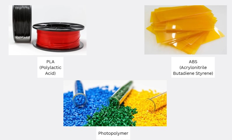
Insulating Materials for 3D Printed PCB Substrates
Conductive Materials for 3D Printed PCB Traces
Conductive paths are typically printed using:
● Silver nanoparticle inks – high conductivity, widely used, compatible with curing via heat or UV.
● Copper inks – excellent conductivity but limited availability and more challenging processing.
● Carbon-based conductors – lower cost, easier to print, but higher resistivity.
Selection depends on current, voltage, and frequency requirements, as well as printer compatibility.
Conductive Materials for 3D Printed PCB Traces
Thermal and Electrical Material Limitations
Engineers must account for material properties that affect performance:
● Glass transition temperature (Tg): sets maximum operating temperature.
● Dielectric loss: affects signal integrity, especially in RF/high-speed circuits.
● Long-term stability: UV exposure, humidity, and mechanical stress can degrade performance over time.
Careful material choice ensures the 3D printed PCB is functional, reliable, and suitable for its intended application.
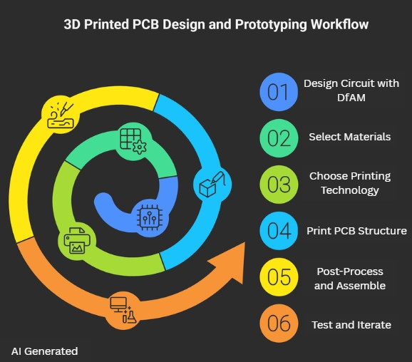
3D Printed PCB Design and Prototyping Workflow
Designing and prototyping a 3D printed PCB follows a workflow that is fundamentally different from traditional FR-4 PCB development. While the overall stages—design, fabrication, assembly, and testing—remain familiar, additive manufacturing introduces unique constraints and opportunities that engineers must account for from the very beginning.
Below is a typical engineering workflow for 3D printed PCB prototyping, optimized for rapid iteration rather than mass production.
1. Design the Circuit with Additive Manufacturing in Mind (DfAM)
The workflow begins with circuit design using Electronic Design Automation (EDA) tools. However, unlike conventional PCB design, Design for Additive Manufacturing (DfAM) plays a central role.
Key considerations include:
● Trace geometry: Printed traces are generally wider and thicker than etched copper. Typical trace widths range from approximately 0.2–0.5 mm, depending on printer resolution and material.
● Layer structure: Multilayer designs are possible but limited, and vias are often replaced by vertical conductive channels or external interconnects.
● Signal integrity: For high-speed or RF designs, impedance control (e.g., 50 Ω) is more challenging due to the dielectric variability of printed polymers. Electromagnetic simulation is often required.
Because most EDA tools are not natively designed for volumetric electronics, the workflow usually involves ECAD–MCAD co-design. Circuit data is translated into a mechanical CAD environment, where conductive paths and insulating structures are modeled in three dimensions before exporting to additive manufacturing formats such as STL or AMF.
2. Select Materials Before Finalizing the Printing Process
In 3D printed PCB development, material selection often precedes process selection, not the other way around.
Material compatibility largely determines which printing technologies can be used and what level of electrical and thermal performance is achievable.
● Insulating Materials: In the case of polymers, PLA or ABS are the ones most widely used. One thing that engineers have to consider quite carefully is the thermal stability—PLA, for instance, breaks down at just above 60 °C, thus the operating environment of the board is very much constrained.
● Conductive Materials: Silver-based nanoparticle inks are the most widely used due to their printability and chemical stability. However, their electrical conductivity is typically several times lower than bulk copper, depending on curing conditions, porosity, and trace geometry.
3. Choose an Appropriate 3D Printing Technology
Once material constraints are defined, engineers can select a suitable additive manufacturing method based on resolution, cost, and complexity.
● Inkjet or Aerosol Jet Printing: Since the methods of direct-writing provide very high precision and thus to conducting fine traces (often not more than 0.1mm), special inks will be laid down (often as small as 0.1mm), making them suitable for sensors, antennas, and RF prototypes. They are primarily used in research and advanced prototyping environments.
● FDM with Conductive Filaments: Fused Deposition Modeling offers a low-cost entry point but produces traces with relatively high resistivity. This approach is best suited for educational use, proof-of-concept models, or low-current functional demonstrations, rather than signal routing or power delivery.
● Substrate-first printing with post-filled conductors: In this approach, the insulating structure is printed first, followed by filling or plating of conductive channels. It offers better conductivity than most conductive filaments and does not require multi-material printers, at the cost of additional post-processing steps.
4. Print the 3D Printed PCB Structure and Conductive Paths
Configuration: Parameters like layer height (usually 0.1 mm to 0.2 mm) and speed of printing are optimized for maximum efficiency. Dual-material printers are a must since they have to alternate between insulating and conductive materials.
It is important to note that multi-material printing is not mandatory. Many workflows separate structural printing and conductor deposition into distinct steps. Regardless of the method, alignment accuracy is critical, as misalignment between layers or channels can result in open circuits or unintended shorts.
5. Post-Processing and Component Assembly
Post-processing follows after the print job in order to have the board ready for the final assembly of components. Post-processing is essential to achieve functional electrical performance.
● Curing: To achieve the highest level of conductivity, conductive inks must be cured in one of two ways, either with heat or UV light, to fuse the metal nanoparticles.
● Component Soldering: Surface Mount Devices (SMDs) are soldered to the paths. As the polymer substrates are unable to tolerate the high temperature (during soldering, usually over 200 °C) so extreme caution needs to be taken in order to avoid deformation.
Thus, engineers often rely on:
1. Low-temperature solder alloys
2. Conductive adhesives
3. Press-fit or embedded component techniques
These assembly methods reflect one of the key differences between 3D printed PCBs and traditional FR-4 boards.
6. Test, Validate, and Iterate Rapidly
Testing focuses on functional validation rather than strict production-level metrics.
● Electrical testing: Continuity checks, resistance measurements, and basic signal verification are commonly performed. Absolute resistance values may be higher than those of copper traces and are evaluated relative to design expectations rather than fixed thresholds.
● Iteration: One of the main advantages of 3D printed PCBs is rapid iteration. Design changes can be implemented quickly in the digital model, printed within hours, and re-tested without external fabrication delays.
This fast design–build–test loop makes 3D printed PCBs especially valuable for early-stage development and complex geometric experimentation.
3D printed PCB prototyping workflow
Pros and Cons of 3D Printed PCBs
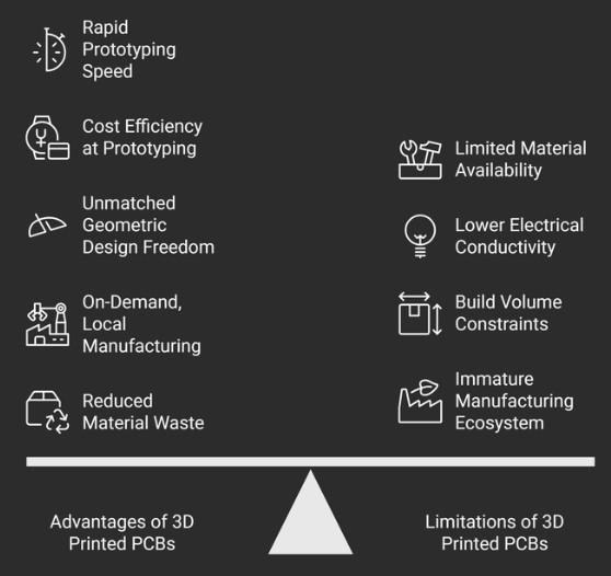
Advantages of 3D Printed PCBs
● Rapid Prototyping Speed: Small-scale 3D printed PCB prototypes can often be produced within hours, significantly shortening design–test–iteration cycles compared to outsourced PCB fabrication.
● Cost Efficiency at the Prototyping Stage: By eliminating external fabrication, tooling, and logistics costs, 3D printed PCBs can reduce expenses for early-stage prototyping and design validation.
● Unmatched Geometric Design Freedom: Unlike planar FR-4 boards, 3D printed PCBs enable non-planar and volumetric circuit routing, allowing electronics to conform to complex shapes and integrate directly into mechanical structures.
● On-Demand, Local Manufacturing: Designs can be manufactured as needed, reducing inventory requirements and minimizing dependency on external supply chains during development.
● Reduced Material Waste: Additive manufacturing deposits material only where needed, resulting in significantly less waste compared to subtractive PCB processes.
Limitations of 3D Printed PCBs
● Limited Material Availability: Most commercial 3D PCB printing systems support a restricted set of proprietary insulating and conductive materials, which can increase costs and limit design flexibility.
● Lower Electrical Conductivity: Printed conductive materials generally exhibit higher resistivity than copper, limiting their suitability for high-current, high-frequency, or low-loss applications.
● Build Volume Constraints: PCB size is restricted by the printer’s build chamber, making large-format boards impractical without modular or segmented designs.
● Immature Manufacturing Ecosystem: Compared to traditional PCB fabrication, the 3D printed PCB equipment market is still small, with fewer vendors and limited process standardization.
Pros and Cons of 3D printed PCBs
3D Printed PCB Applications and Use Cases
1. High-Frequency and RF Systems
At high frequencies, traditional planar PCBs often face design constraints when dealing with complex RF geometries, impedance transitions, and antenna integration—especially in compact or non-planar devices. While mature RF laminates still offer superior and predictable dielectric performance, additive manufacturing enables new RF design possibilities that are difficult to achieve with conventional PCB fabrication.
Key use cases include:
● Conformal and Integrated Antennas
Antennas can be directly printed onto curved enclosures or structural surfaces, enabling conformal antenna designs that reduce assembly complexity and improve space utilization in RF modules, wearables, and compact wireless devices.
● Rapid RF Prototyping and Geometry Optimization
3D printed PCBs allow fast iteration of transmission lines, waveguides, and antenna structures, making them well suited for early-stage RF prototyping, low-GHz applications, and experimental designs where form factor and geometry play a critical role.
Note: Due to current limitations in dielectric consistency and loss control, 3D printed RF circuits are primarily used for prototyping, antenna structures, and non-critical RF paths rather than high-volume, high-precision RF production.
2. Medical and Wearable Devices
Medical and wearable electronics demand compact form factors, customization, and mechanical flexibility—areas where 3D printed PCBs offer clear advantages over rigid, planar circuit boards.
Typical applications include:
● Flexible Biomedical Sensors
Thin polymer-based substrates can be printed to conform to the human body, enabling lightweight, wearable sensors for external or short-term biomedical monitoring such as motion tracking, physiological sensing, or rehabilitation devices.
● Integrated Electronics for Prosthetics
Control electronics can be embedded directly into the structural components of prosthetic limbs or assistive devices, reducing overall system bulk while improving aesthetic integration and mechanical robustness.
Note: Most current applications focus on non-implantable or short-duration contact devices. Long-term implantable use remains largely experimental due to biocompatibility, reliability, and regulatory constraints.
3. Aerospace and UAV Systems
In aerospace engineering, reducing weight, simplifying assembly, and accelerating development cycles are constant priorities. 3D printed PCBs enable tighter integration between structural components and electronic systems, particularly in low-volume or experimental platforms.
Representative use cases include:
● Embedded Conductive Pathways in Structural Parts
Conductive traces can be integrated into 3D printed ribs, panels, or housings, reducing the need for traditional wiring harnesses in small satellites, experimental payloads, or space-qualified prototypes.
● Rapid Prototyping for UAV Electronics
For unmanned aerial vehicles (UAVs), sensor boards and control electronics can be rapidly redesigned and printed to match aerodynamic shells or custom airframes, significantly shortening development and testing cycles.
Note: These applications are most common in small satellites, research platforms, and rapid prototyping environments rather than long-life, mass-produced aerospace systems.
4. Integrated Sensor Systems and IoT Devices
In many IoT applications, the ideal outcome is seamless integration—where electronics blend into the physical environment instead of existing as separate assemblies.
Key applications include:
● Structure-Integrated Sensors and Controls
Sensors, interconnects, and low-power control circuits can be printed directly onto or within product housings, smart furniture, lighting fixtures, or industrial enclosures, reducing the number of discrete PCBs and connectors.
● Compact, Custom IoT Prototypes
By consolidating structural and electronic functions, 3D printed PCBs enable rapid development of customized IoT devices with fewer mechanical constraints and simplified assembly workflows.
Rather than completely replacing traditional PCBs, additive manufacturing is most often used to reduce PCB count, simplify system architecture, and enable form factors that conventional fabrication cannot support.
JLCPCB's Role in Practical 3D Printed PCB Prototyping
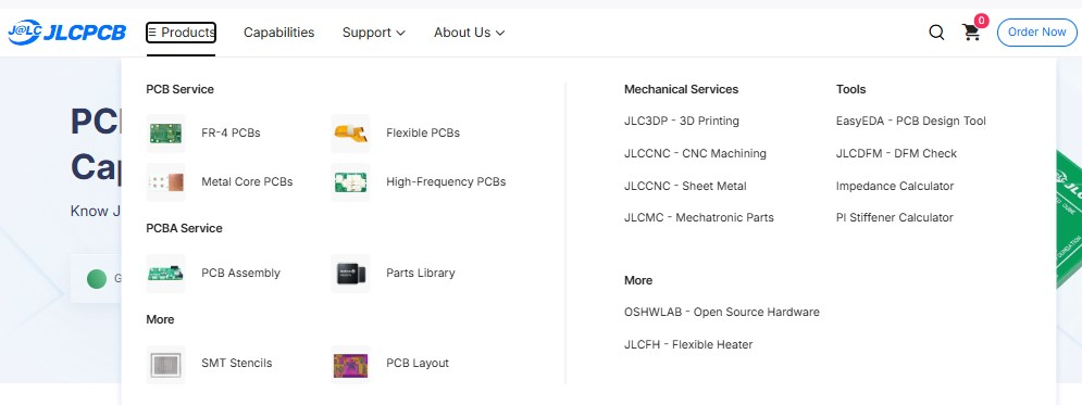
JLCPCB provides a fast and reliable pathway for engineers to turn designs into real hardware. They focus on quality control of industrial-grade traditional PCBs, including multi-layer FR-4 and aluminum-core boards, among others, and deliver them in a quick and cost-effective manner. With EasyEDA, engineers can design circuits online and directly order PCB fabrication and assembly, creating a smooth end-to-end workflow.
The assembly services offered by JLCPCB are for both rigid and flex printed circuit boards. They are supported by each DFM check and AOI inspection, which helps in minimizing defects and ensuring professional-quality results. Thus, the process is not only suitable for prototyping but also for small-scale production.
Fully 3D-printed PCBs are still at a very early stage of development in research labs, whereas the practical method of today is a hybrid one: electrical performance is achieved through traditional PCBs, and 3D-printed parts are used for custom mechanical design. JLCPCB is in a position to facilitate this through JLC3DP, its exclusive 3D printing service for making enclosures, brackets, and structural components from materials such as PLA and ABS.
This combination lets engineers fabricate a high-quality PCB while simultaneously ordering tailored mechanical parts, resulting in well-integrated prototypes without sacrificing electrical reliability.
Together, JLCPCB’s PCB manufacturing, assembly, EasyEDA design tools, and JLC3DP services offer a complete ecosystem for bringing ideas into working prototypes or early production.
Note: JLCPCB currently provides traditional PCB manufacturing and separate 3D printing services—not fully 3D-printed PCBs.
PCB Manufacturing and Assembly Services of JLCPCB
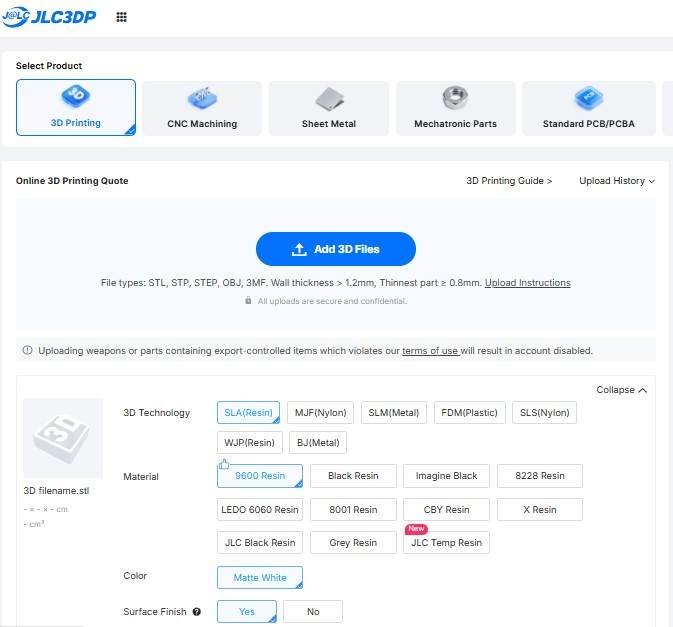
3D printing service with JLC3DP
Conclusion
3D printed PCBs represent a fundamentally different approach to electronic design, enabling circuits to be integrated directly into three-dimensional structures rather than mounted on flat boards. This capability opens new possibilities for conformal electronics, structural integration, and rapid prototyping that are difficult or impossible to achieve with traditional FR-4 PCBs.
While current limitations in material conductivity, thermal performance, and manufacturing scalability remain, ongoing advances in conductive inks, dielectric polymers, and printing resolution continue to improve practical performance. As these technologies mature, 3D printed PCBs are expected to play an increasingly important role in prototyping, customized electronics, wearables, IoT devices, and complex geometric applications, complementing—rather than replacing—traditional PCB manufacturing.
FAQ about 3D Printed PCBs
Q1 Can you 3D print a circuit board?
Yes, a circuit board can be 3D printed, but with important limitations. 3D printed circuit boards are created using additive manufacturing techniques to build the board structure and conductive traces layer by layer, rather than etching copper on FR-4. While this approach works well for rapid prototyping, conformal electronics, and custom geometries, it does not yet match traditional PCBs in conductivity, thermal performance, or scalability for mass production.
Q2 Are 3D printed PCBs strong enough to replace traditional FR-4 boards in real products?
Yes, but only in some specific situations. 3D printing substrates of plastics such as ABS or some special photopolymers make it possible for prototypes, wearables, IoT enclosures, and lightweight aerospace parts to be very strong mechanically. Notwithstanding, they cannot yet be compared with FR-4 in terms of mechanical strength, temperature resistance, and long-term reliability for high-power consumer electronics or industrial systems. Currently, engineers use 3D-printed PCBs mainly for structural-functional prototypes or for low-stress product categories.
Q3 Can conventional electronic components (SMD, through-hole) be directly used on 3D printed PCBs?
Yes, standard components can be mounted on 3D-printed PCBs, but with limitations. Polymer substrates may deform under high soldering temperatures, so designers typically use:
● Low-temperature solder alloys,
● Conductive adhesives, or
● Cold-soldering techniques.
The through-hole parts could be held in position by printing reinforced vias or by inserting metal-plated inserts. The essential aspect is to make sure that the thermal stress does not cause any distortion to the substrate.
Q4 How do 3D printed PCBs affect electromagnetic performance, especially for RF circuits?
3D-printed materials often have higher dielectric losses and less predictable EM properties than traditional substrates. This situation in the RF applications could bring problems like shifting of the frequency, higher signal attenuation, and the reduction of the antennas' efficiency.
On the other hand, the 3D printing technique allows for custom dielectric shaping, which is, in fact, the opposite of what is done in flat PCBs, and thus it could trigger significant RF performance improvements if such designs are done right. They often employ computational EM simulations to optimize these unique geometries.
Q5 Are 3D printed conductive inks safe and stable over time?
Most conductive inks—especially silver nanoparticle inks—are chemically stable when properly cured. However, their long-term electrical stability depends on environmental conditions:
● High humidity can cause oxidation or slight resistivity drift.
● Mechanical stress can lead to micro-cracking in the printed traces.
● UV exposure may degrade some polymer-based inks.
To improve longevity, designers often coat the printed circuits with conformal coatings or encapsulate the entire structure.
Q6 Is the mass production of 3D printed PCBs economically viable?
Not at present. Even though 3D-printed PCBs stand out in rapid prototyping, custom geometries, and low-volume special-purpose manufacturing, their production speed and material costs still render them unfit for large-scale manufacturing. Traditional PCB factories still outperform in:
● Cost per unit
● Production speed
● Yield rate
● Material precision
3D printing is expected to complement—not replace—traditional PCB mass production in the near future.
Q7 Can 3D Printed PCBs Be Manufactured at Scale?
At present, large-scale manufacturing of 3D printed PCBs is limited. While the technology supports automation and digital workflows, current constraints in printing speed, material cost, equipment availability, and process consistency prevent it from competing with traditional PCB fabs at scale. Today, 3D printed PCBs are best suited for low-volume production, customized designs, and rapid prototyping, rather than high-volume standardized manufacturing.
Keep Learning
PCB Assembly for Wearable Devices: Tips, Materials, and More
Wearable electronics — including health monitors, smartwatches, AR/VR headsets, and biosensors — represent one of the most transformative innovations in consumer and medical technology. These compact systems are engineered to deliver high functionality, user comfort, and long operational life simultaneously. This combination creates unique requirements for the printed circuit board assembly (PCBA) at its core. Unlike traditional rigid boards, PCBs used in wearables must be exceptionally thin, lightwei......
Integrating Raspberry Pi with PCB Design for Cutting-Edge Projects
Introduction The Raspberry Pi has revolutionized the world of electronics with its affordability and versatility. When combined with PCB (Printed Circuit Board) design, it offers a range of exciting possibilities for hobbyists and engineers alike. This article dives into how Raspberry Pi in PCB design is transforming the landscape of electronics. From integrating Raspberry Pi into custom PCBs to exploring advanced projects, we’ll guide you through practical tips and insights on Raspberry Pi Integratio......
Arduinos and PCBs Comprehensive Integration Guide
Introduction In the realm of electronics, the Arduino PCB is a vital component for enthusiasts and professionals alike. The Arduino microcontroller platform has revolutionized PCB design for Arduino, allowing for unique and customizable Arduino circuit designs. By integrating Arduino with PCBs, you open up a world of possibilities for creating specialized electronic devices. This article delves into the integration of Arduinos with PCBs, focusing on Arduino circuit design, the creation of custom Ardui......
Discover the Power of ESP32 Microcontroller Projects
The ESP32 microcontroller is a favorite among tech enthusiasts for its amazing features and versatility. It boasts a dual-core processor, Wi-Fi, and Bluetooth, making it ideal for various DIY and professional projects. In this article, we'll look at some exciting ESP32 projects, from home automation to environmental monitoring that will show you how to make the most of this microcontroller. Home Automation with ESP32 Home automation is one of the most popular uses for the ESP32. Its built-in Wi-Fi and......
3D Printed PCB Explained: Technology, Materials, Pros, Cons, and Applications
3D printed PCBs are redefining how electronic circuits can be designed, prototyped, and integrated into complex structures. Unlike traditional FR-4 boards, this additive manufacturing approach enables conformal geometries, structural electronics, and rapid iteration without tooling or chemical etching. This article explains what 3D printed PCBs are, how they work, their key advantages and limitations, and how they compare to conventional PCBs—helping engineers and product designers understand when thi......
Comprehensive Guide to the ESP32 Microcontroller Powering IoT Innovations
Introduction The ESP32 microcontroller has rapidly become a cornerstone in the world of IoT (Internet of Things), providing developers and hobbyists with a versatile, powerful, and cost-effective platform. This article delves into the definition of ESP32, its usage in various applications, and provides examples to highlight its capabilities. With its robust feature set, the ESP32 is not just another microcontroller but a game-changer in the IoT landscape. ESP32 Definition: The ESP32 is a low-cost, low......