Mastering Precision in PCB Drilling : Tools, Techniques, and Via Optimization for High-Quality Boards
15 min
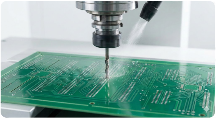
In the modern multilayer boards, the accurate holes are used to connect internal copper layers and to assemble components. In our case, the drilling opens the vias and through-holes through which the signals are transferred among the layers, and it is the most important part of the PCB manufacturing, frankly speaking. The reason is that it provides the basis of vias and ensures that the various PCB layers are able to communicate with one another. All through-holes on the plated begin as a simple drilled hole which is then coated with copper. A hole that is as small as 100um in diameter must strike the mark. You make those holes wrong and you get open circuits or interconnections that are flaky and the entire board is affected. The quality of boards, signal integrity, and final assembly is basically based on drilling.
Non-electrical holes should also be dealt with by efficient drilling. Other holes remain unplated so that screws or alignment fixtures can be mounted. In all of them, the drill must pierce a clean and perfectly centred hole of the correct size. In the current PCB production all boards are handled like a large drill worksheet, and any minute movement is unacceptable. This is the reason why correct drill drawings and files are important- they allow the CNC machines to know the exact location of each hole to be drilled.
The Essential Role of Drilling in Interlayer Connectivity
Drilling in PCBs is therefore what essentially allows those electrical connections to occur. With a multilayer board, you can have 4, 6 or more copper layers - without those holes of the drilled board, all the layers would be individual islands. Through-holes and vias become the connections that bind it all together. Once you have drilled you plate up the holes so that copper may actually run through the board. The drill bit then clears the neighborhood of the signals basically. The hole, when plated up, forms a copper-lined barrel, where the power and data can be shot either up or down.
That connectivity is super critical when you move into high density boards. Similar to smart phones, a multi-layer board can contain thousands of vias. Each of them must connect with copper pads and traces on every layer in a perfect manner to achieve a seamless connection. According to one industry expert, drilling must be precise - if it is not, the machine will not even fit on the board since the holes will not line up correctly.
Differences Between Through-Holes, Blind Vias, and Buried Vias
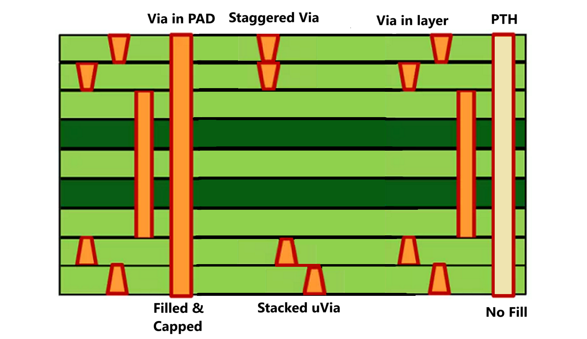
- Through-Hole (Plated Through-Hole, PTH) – The most common via on PCBs, a through-hole is drilled completely through the board from top to bottom. After plating, it electrically ties all layers together. Through-holes are used for standard via connections and through-hole component leads. They guarantee a continuous connection through the entire thickness of the board.
- Blind Via – A blind via connects an outer layer with one or more inner layers, but does not exit the other side of the PCB. From the outside, it looks like a partial drill or blind because you can’t see through it. Blind vias save space in HDI designs. They allow outer-to-inner-layer connections without consuming board real estate on the far side, which is vital when cramming a lot of circuitry into a small area.
- Buried Via – A buried via is entirely inside the board, connecting internal layers only. You won’t see it from the outside at all, because it’s buried between the cores. Buried vias enable extremely dense multilayer designs by freeing up surface space. However, they require drilling and plating inner layers before the final lamination step, making them more complex to manufacture.
Additional note: Microvias are ultra-small blind vias (often <0.15 mm) created by laser drilling. These are used in modern HDI boards for super-fine connections, especially between adjacent layers. Laser drills make microvias so small and precise that they wouldn’t be practical with mechanical drills.
Advanced Drilling Tools and Equipment in Modern Fabrication
At PCB plants, we tend to use glitzy CNC drilling machines as opposed to those bulky hand-held tools. The current machines have the ability to rotate at ridiculous speeds (150,000 RPM on air spindles) and thus can cut holes as small as 100 microns. JLCPCB even boasts that! And guess what? Even the finest dental drill will only go to approximately 40,000 RPM, and those CNC machines are well beyond that. These spindles which are air-bearing are capable of switching between holes in a super-fast fashion, producing hundreds of holes per minute with a precision of microns. In consistency, it is simply a no-brainer, no human hand can match that robotic drill of 150k RPM.
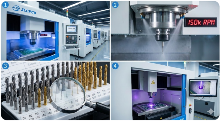
Besides sheer speed, advanced drills include automatic tool changers and laser drill attachments. High-end lines often integrate both mechanical and laser drilling in one cell. JLCPCB notes it uses advanced CNC drilling machines, laser systems, and strict quality control to ensure precision in every hole. The CNC machines handle the bulk of standard via and component holes, while UV or CO₂ lasers tackle the microvias and blind vias that require sub-millimeter precision. By combining tools, manufacturers cover every hole diameter and type needed for modern boards.
High-Speed Spindles and CNC Drilling Machines
The key feature of PCB drills is high rotational speed. Spindle speeds for PCB work are tens of thousands of RPM much higher than metalworking drills. High speed keeps chips small and reduces thrust force, which is vital when penetrating glass-fiber substrates. For example, IPC guidelines suggest 40,000–60,000 RPM for holes around 0.5 mm diameter, with even higher speeds for microvias. Many machines use air bearings at the tip to minimize vibration and allow speeds above 100,000 RPM when needed. The drill’s high-speed precision means it can produce 0.1 mm holes reliably, a must for high-density boards.
CNC automation is, truly, a life-saving tool since it is all literally on rails. The board remains attached to the machine and the computer is merely following the drill program to pull the head and create every hole. Precision XY tables and stepper motors ensure that every hole is placed precisely where it is required to, typically a matter of micrometers. It is very good news to PCB designers-they will be sure that the factory will punch holes where they need them. Bonus, repeatability of quality: each board within a particular batch is drilled exactly the same way.
Drill Bit Types: Carbide, Geometry, and Coating Variations
PCB drilling is not only about the fancy machines, but it is all about the drill bits. Majority of the holes of a PCB are drilled using solid tungsten carbide bits since these bits are extremely difficult and remain sharp as they cut through fibrous FR-4 glass. Carbide can last up to ten times longer, and much fewer defects can be made compared to HSS. HSS bits are nearly never applied to commercial PCBs as they wear out quickly and disrupt the hole quality.
No less important is the geometry of the drill. The PCB drills are typically set at a point of 130-140 degrees of point to cut the thrust and leave a clean entry and exit on laminates. The length of the flute, the angle of the helix and the thickness of the web are all adjusted to achieve rigidity and chip removal. In the case of microvias (less than 0.2 mm), centralization and breakage prevention is done with specially ground microdrills that nail the microvias. PCB drills are coated with TiN or diamond-like coats to reduce friction and wear, particularly in ultra-fine holes. The same coatings increase the life of the tool, enhance the quality of the hole and reduce the cost of tooling.
Laser Drilling as a Complementary Precision Option
I believe that mechanical carbide drills are perfect on most holes, but when the vias become extremely tiny, laser drilling usually takes over, and it is a rather cool idea that the laser does not have to touch the material to cut it. The technology of laser drilling has gained popularity. A microvia (0.02 mm) can be created using a UV laser to punch through a thin layer of copper/resin and a CO 2 laser can pierce through a more robust layer of resin.
They are slower with large volumes, and do not cut thicker copper foil, and thus are a supplement, not a substitute, to mechanical drills. Laser equipment is very expensive and therefore is normally only utilized in high-density designs where microvia reliability is paramount. In practice, an HDI board might see mechanical drills do all >0.15 mm holes, while lasers handle the sub-0.15 mm microvias between BGA pads. The end result is an ultra-fine interconnect network that mechanical bits alone couldn’t achieve. Engineers can specify laser-compatible via sizes, knowing the manufacturer has laser capability.
Key Techniques for Accurate and Efficient Drilling
Stack Height Management and Drill Depth Control
Manufacturers tend to stack a number of boards to increase throughput. But, piling up the boards under a single bit may be detrimental to accuracy. The practice of the industry is to restrict the stack height to a maximum of 3 to 5 boards of 1.6mm FR-4. Quarantine may exceed this resulting in deflection and increase position tolerance error. In order to cope with this, fabricators employ entry/exit media. They place the board stack between sheets of protection on the top and bottom of the stack- a top entry layer and bottom exit layer. The exit sheet receives the drill at the base and the entry sheet directs the drill tip on the top surface minimizing the tear-out and burrs.
In case of controlled-depth drilling, the contemporary drills have the capability to trace the depth. A blind hole of the appropriate depth will be left behind with the bit being retracted by the CNC after a specified distance. The process of making blind vias is as follows: the drill does not penetrate to the copper inner layer, but is reversed, and exits at the inner copper layer. Controlled depth drilling is not well calibrated but enables to drill precise internal holes without endangering the outer layers.
Peck Drilling and Chip Removal Strategies
When I am drilling FR-4 or other fiberglass boards the flutes of the drill may be clogged with resin and glass chips. A peck method of drilling is employed in many machines: the bit sets forward a little, sets back a little, and so on. The chips are broken up by that cycle and pushed out with the help of airflow to maintain the temperature. Moreover, a vacuum or high-pressure air is typically blown past the spindle to blow away chips off the bit. In high volume lines automated vacuums or brushes sweep the panel between drill steps. Removal of the chip is important - in case the bit becomes stuck, it may burn or become off-centered.
The dust control is also completely essential. FR-4 dust is fine and coarse. Many stores bore holes in it and then blow it off with a compressor or vacuum. Others go to the extreme to employ a mist-cooling system, a fine spray of oil or aerosol to cool the bit and control dust without misting the board. Ultimately, the drills are based on peck cycles, air blasts, and vacuum extraction to maintain the cutting area clean. This keeps it from getting hot and is also crucial in making sure that every hole is accurate- even when you are doing thousands of them.
Optimizing Drilling Parameters for Board Quality
- Spindle Speed (RPM): Higher RPM makes the drill bit cut faster, reducing cutting force. PCB drills run at much higher speeds than metalworking drills. For instance, IPC guidelines suggest up to 80,000–100,000 RPM for holes below 0.5 mm. One rule-of-thumb: smaller holes need higher RPM.
- Feed Rate: This is how fast the drill advances downward (typically in inches or mm per minute). The critical parameter is chip load: how much material is cut per revolution. For standard FR-4, a chip load of about 0.001–0.002 inches per revolution is common.
- Hit Count Limits: Every drill bit has a finite life. As it wears, hole quality degrades (more burrs, rough walls). IPC-DR-572 gives typical durability numbers: a fresh bit can drill about 3,000–3,500 holes in double-sided FR-4 before regrinding.
Feed Rates, Spindle Speeds, and Hit Count Limits
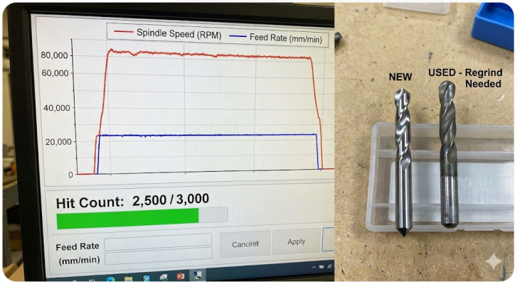
As noted, balancing RPM and feed is key. FR-4’s composition (fiberglass + resin) is abrasive and heat-sensitive. Higher speeds reduce thrust but increase heat; higher feed increases material removal but loads the bit. A common strategy is to start with moderate values, then tune. Many PCB drilling guides emphasize chip load consistency. Modern CNC controllers can dynamically adjust RPM and feed to maintain a target chip load. Hit count monitoring is enforced in high-end shops. For example, after each regrind of a carbide bit, the flutes shorten meaning it can’t drill as many boards in a stack without deflecting.
Minimizing Burrs, Hole Wall Roughness, and Plating Voids
Even with perfect positioning and sharp tools, drilling can introduce defects: burrs at entry/exit, rough walls, or tiny gaps where plating might not adhere. Several strategies mitigate these. First, using entry and exit backing material (as mentioned above) dramatically cuts burrs on the top and bottom of the board. Second, the drill’s cutting parameters impact wall smoothness.
After drilling, a light de-burring pass or brushing can remove residual roughness. Some shops use a secondary process: backdrilling (running a bit from the bottom side partway up) to eliminate plug-shaped nails in buried vias, or an ultrasonic cleaning to clear out dust. This prevents plating voids areas where copper doesn’t fully coat the hole wall. Good drill practices and bit maintenance go a long way here.
Thermal Effects and Material-Specific Adjustments
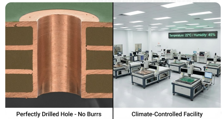
Temperature also matters in terms of thermal expansion. If the shop environment is too warm or humid, the PCB stack could expand slightly, throwing off registration. Good facilities control climate carefully. Some manufacturers even pre-bake boards to remove moisture before drilling, especially for materials like FR-4 which absorb humidity. A FR-4 stack might use air-blow dust control, while a ceramic-filled board might use mist cooling. Engineers should provide the board material (FR-4, polyimide, etc.) so the fabricator can adjust parameters.
Challenges in PCB Drilling and Professional Mitigation
Common Defects Like Misalignment and Breakage

Misalignment between layers is a top concern. If a drill shifts or the board drifts, a via might miss its target pad or skew, causing opens. Stack misalignment can occur if the board panels aren’t perfectly flat, or if too many layers cause a “tenting” effect. To combat this, manufacturers tightly clamp panels and use thin support films, ensuring that each board lies flat.
Drill breakage is another worry. Tiny carbide bits, especially under 0.3 mm, are quite fragile. A sudden dive into a trapped board corner or a mis-set feed could snap one. To mitigate this, drills are programmed with breakage protection: if current spikes or position feedback shows an unexpected jerk, the machine halts. Bits are also inspected after every job (often under a microscope) for wear or cracks.

Frequently Asked Questions (FAQ)
Q: Why are PCB drilling accuracy and hole quality so important?
A: Because every via starts as a drilled hole, and any error affects electrical connectivity. Inaccurate or rough holes can lead to poor plating, increased resistance, or open circuits.
Q: How do I specify hole requirements when ordering a PCB?
A: In your fabrication notes or drill drawing, list the diameter and plating status for each hole. If you need a particular kind of via (blind, buried, microvia), mention that and ensure the manufacturer has the capability.
Q: Can I use the same drill program for multiple boards stacked together?
A: Yes, that’s a common practice. The same drill coordinates can apply to every board in the stack, saving setup time. Just be mindful of stack height limits: usually 3–5 standard boards per stack.
Q: What materials can I drill? Does it differ from standard FR-4?
A: FR-4 is the standard and what most fabricators optimize for. You can also drill other materials (polyimide, Rogers, ceramic, metal-core), but the parameters change.
Q: How long does the drilling process take in PCB manufacturing?
A: Surprisingly, even though drills spin at 100k+ RPM, drilling isn’t instantaneous. A large, complex panel might have hundreds of holes.
Q: What are JLCPCB’s drilling capabilities?
A: JLCPCB can handle multilayer PCBs up to 12 layers, with blind and buried vias by request. We routinely drill holes down to 0.1 mm (4 mil) and use laser drills for microvias in HDI boards. Their machines reach 150,000 RPM and maintain hole positional tolerances of a few microns.
Keep Learning
PCB Etching in Professional Fabrication : Modern Techniques and Industrial Strength
The etching of printed circuit boards is the selective removal of unwanted copper on a board to form the conductive traces and pads. It is effectively a subtractive process; after the photolithography or a printed resist mask has been applied, the remaining copper is removed with a chemical ether solution. It leaves the circuit pattern it was intended to create. Well, imagine that you are on the copper at the spa, you put it in the correct bath, and the undesired metal just dissolves. Etching is accur......
Mastering Precision in PCB Drilling : Tools, Techniques, and Via Optimization for High-Quality Boards
In the modern multilayer boards, the accurate holes are used to connect internal copper layers and to assemble components. In our case, the drilling opens the vias and through-holes through which the signals are transferred among the layers, and it is the most important part of the PCB manufacturing, frankly speaking. The reason is that it provides the basis of vias and ensures that the various PCB layers are able to communicate with one another. All through-holes on the plated begin as a simple drill......
Laser Engraving vs. Professional PCB Fabrication : Understanding DIY Limitations and Industrial Advantages
In the conventional approach, we first apply a mask pattern and then remove metals using chemicals. In hobby electronics, using a laser engraver to make circuit boards is an exciting idea. The basic concept is to generate a laser to pattern a copper-clad board. Typically, a bare PCB is first coated with a dark resist layer that protects the copper. Then a laser cutter follows your circuit design to burn away the resist where copper traces should remain. After laser etching, the exposed copper is chemi......
The Significance of Industrial PCB Manufacturing for Modern Technology
Industrial PCB manufacturing is an important part of making strong printed circuit boards (PCBs) for high-performance tools in many fields. Industrial PCBs are different from regular consumer electronics because they are made to work in severe environments, be reliable over time, and meet specific operating needs. These PCBs are very important for things like computer systems, heavy machinery, medical equipment, and the infrastructure for energy production. 1. What Is Industrial PCB Manufacturing? Whe......
Process of PCB Production
Modern electronics are built on printed circuit boards (PCBs), which also provide the platform connecting and running almost every electronic device, from industrial equipment to cellphones. PCBs have transformed the way that electronic components are combined to enable the creation of more dependable, small, and potent devices. Considering all of the steps involved, different types of PCBs, and their uses across sectors, this article covers the complex process of PCB production. What is PCB Productio......
The Science Behind PCB Silkscreen Inks and Printing Techniques
Have you ever wondered what type of processes are used in PCB fabrication so that they have permanent silkscreen? How does this ink not erase even if under very harsh conditions? By the way, silkscreen is the top-most layer of a PCB, the white legends that consist of component labels, logos, and polarity marks. Today, we will see the chemistry behind all this and know what type of printing technology is required to make them work. Behind these clean white lines lies a fascinating combination of materi......