
Laser Engraving vs. Professional PCB Fabrication : Understanding DIY Limitations and Industrial Advantages
14 min
- Technical Process and Material Considerations in Laser Engraving
- Limitations and Challenges of DIY Laser Engraving for PCBs
- How Industrial PCB Fabrication Outperforms Laser DIY Approaches
- When Professional Manufacturing Is the Better Choice
- Frequently Asked Questions (FAQ)
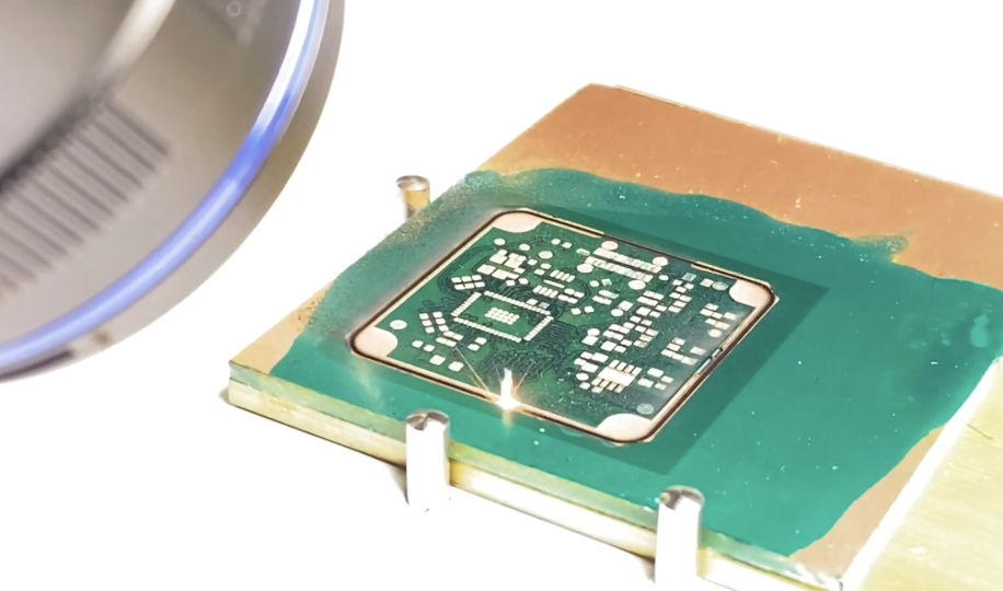
In the conventional approach, we first apply a mask pattern and then remove metals using chemicals. In hobby electronics, using a laser engraver to make circuit boards is an exciting idea. The basic concept is to generate a laser to pattern a copper-clad board. Typically, a bare PCB is first coated with a dark resist layer that protects the copper. Then a laser cutter follows your circuit design to burn away the resist where copper traces should remain. After laser etching, the exposed copper is chemically etched away. First, paint the PCB black. Then, engrave the isolation contours of the tracks. Finally, etch the freed copper. In other words, the laser performs the masking step that photolithography or toner transfer normally does.
Basic Principles Behind Laser Etching and Cutting
Laser PCB prototyping is relatively easy to set up. A common approach is to spray a bare copper board with matte-black paint until the copper tracks are no longer visible. You then prepare your circuit file and run the laser. The beam vaporizes the black paint where copper should stay, revealing shiny copper. A quick wipe of the board cleans any burnt paint residue. Finally, the board is immersed in an etchant that dissolves all unmasked copper, leaving only the laser-defined traces.
Another approach uses photo-sensitive resist and a UV/blue laser. Instead of paint, the PCB is laminated with a UV-sensitive film. A 405 nm laser can then “draw” the circuit by exposing the resist directly. This has been shown to produce very fine traces on the order of 0.2 mm lines. After exposure, the board is developed and etched like a conventional photo board. This UV-laser method can yield higher resolution than burning paint, but still requires chemicals to etch away unwanted copper.
Typical Use Cases for Hobbyists and Small-Scale Prototyping
Laser etching has been used to prototype small driver boards for brushless motors. Makers have crafted custom sensor modules and Arduino shield PCBs by laser-etching the trace patterns onto them. A laser cutter is also handy for cutting unusual board outlines or for making PCB stencils. In practice, hobby laser-etched PCBs are usually single-sided or at most simple double-sided boards. They shine in educational or experimental settings where you need a board right now and are willing to sacrifice some polish. Laser-cut masks are perfect for creating really precise masks for even the smallest ICs, making lasers great for fine-pitch hobby projects.
Technical Process and Material Considerations in Laser Engraving
Common Laser Types and Their Interaction with PCB Substrates
DIY laser PCB makers use various kinds of lasers, each with strengths and limitations:
- CO₂ lasers (10.6 μm infrared) are very common in hobby laser cutters. They easily cut organic materials and FR-4, but copper reflects most IR. In practice, a CO₂ laser indirectly patterns a PCB, then it burns through the black paint mask with ease. Many makers use desktop CO₂ machines to do multiple passes at low power until the paint is cleared.
- Diode and blue/UV lasers (400–450 nm) are increasingly popular in the maker world. A small 405 nm or 445 nm diode laser can be mounted on a CNC or 3D printer to engrave PCBs. These shorter wavelengths are better absorbed by copper than IR.
- Fiber/Nd: YAG lasers (1064 nm) and UV lasers (355 nm) are the tools of industrial PCB fabrication. Fibre lasers produce very high power density and are excellent at vaporizing copper. In professional “laser etching” lines, a focused fibre beam can directly remove copper without a mask, allowing for extremely fine detail. These lasers also operate in pulsed mode to ablate copper cleanly. But they use a costly setup.
Key Parameters: Power, Speed, and Focus in Practice
The three key engraving parameters are power, speed, and focus. It must be balanced for best results:
- Power (laser intensity): In most PCBs, you want just enough power to remove the mask without damaging the underlying layers. Very low laser power with multiple passes gives cleaner traces. For example, using a 40 W CO₂ laser, set it to only 4% power and make four passes to etch through the paint. The lower the power, the less heat into the board. If you crank the power too high, you risk burning or charring the substrate. A low-power, multi-pass approach eases through the mask like sandpaper.
- Speed (beam movement rate): Slower speeds mean the laser dwells longer on each spot, removing more material. Per pass, use slower speeds to cut through thicker paint or engrave deeper. The tradeoff is that too slow motion or too high power can overheat FR-4. In practice, using 10% of maximum speed (with low power) was effective on tough enamelled paint.
- Focus (spot size): The laser must be accurately focused on the board surface. A focused beam yields a small diameter spot; a defocused beam creates a larger, weaker spot. Ensure your machine’s focus lens is clean and that the board is flat. If the focus drifts or if the board wobbles, the trace width and depth will vary.
In summary, start with low power + slow speed and adjust. If the laser barely scratches the mask, slow down or increase power a bit. Fine-tuning these parameters usually takes trial runs on scrap before the real board.
Limitations and Challenges of DIY Laser Engraving for PCBs
Precision and Via Quality Issues
While laser engraving for PCBs is clever, there are significant precision and reliability trade-offs:
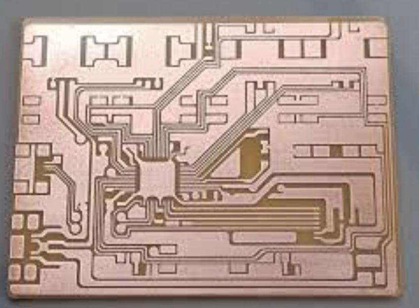
- Trace Resolution: Lasers are nowhere near the industrial photolithography precision. A typical DIY laser spot is on the order of 0.2–0.5 mm, limiting the narrowest trace that can be drawn. In practice, a 405 nm “high-res” laser got 0.2 mm traces. By contrast, professional fabs routinely do 0.10 mm (4 mil) or smaller. JLCPCB, for example, lists a minimum trace/space of 0.10 mm on two-layer boards.
- Vias and Holes: In professional PCBs, vias are made by precise drilling and copper plating. JLCPCB drills holes as small as 0.1 mm (100 µm). Home setups cannot match that. The finest hand drills yield 0.3 mm holes at best, and they are unplated. A drilled hole in a laser-etched board will not have copper plating on its walls, so it doesn’t automatically connect copper on both sides. The laser-etched PCB typically cannot have robust multi-layer vias or plated through holes. Any through connections are low-quality and prone to failure.
Material Constraints and Safety/Environmental Concerns
FR-4 board is made of epoxy resin and fiberglass cloth. Burning or overheating it releases toxic fumes. Even the epoxy smoke produces aldehydes and phenols that are nasty. Adequate ventilation or fume extraction is mandatory. Do NOT run a laser cutter on FR-4 in a closed room without a good exhaust system. Similarly, the spray paint coating also produces fumes and soot when lasered. Even “low-power” diodes (<5 W) emit intense visible/UV light. Never leave a laser unattended while cutting. The PCB project is not worth eye damage! The convenience of not using toxic etchants for laser-only processes must be weighed against inhaling laser smoke. In practice, most laser PCB methods still require some chemical etching, so you’ll have fumes from acids too. It’s a balancing act of safety gear and good airflow.
Scalability Problems for Multi-Layer or High-Volume Boards
True multilayer boards are impossible to design with this technique. There is no straightforward way to lay up multiple patterned layers or to align and bond them like in a lamination press. Some adventurous makers manually glue two single-sided boards together, but the misalignment and lack of inner copper make that an unreliable hack. You cannot laser-passivate inner layers or plate through from home. If your design calls for a 4-layer or 6-layer PCB, only a professional fab can do that. Even for a single-layer board, a large panel exposes limitations. The industrial laser etching processes actually note that it can be hard to etch evenly on large boards. Any tilt or wobble means some areas are under-cut while others are over-burned for dozens of boards in one go.
If you need multiple identical boards, doing them one by one at the laser is painful. A single 50 mm×50 mm board might take 10–20 minutes to engrave and then 30 minutes to etch. If you need 10 boards, that’s hours of machine time plus a chemical bath for each. In contrast, a PCB manufacturer can produce 10 copies simultaneously (or more) with identical quality in about a day of shop time. It is absolutely not suited for tens or hundreds of boards, or for the complexity of multi-layer fabrication.
Long-Term Reliability Risks in Laser-Produced PCBs
Even if a laser-etched PCB works initially, there are long-term concerns:
- Incomplete Copper Removal: Laser masks may leave a thin smear of paint or resist that wasn’t fully removed. Cleaning with isopropyl alcohol is needed to polish away the final film. If that step is imperfect, leftover residue can prevent solder wetting or cause corrosion.
- No Protective Finishes: Commercial boards typically get a soldermask and a finish like HASL or ENIG to protect copper and help with soldering. DIY laser boards usually skip soldermask, leaving bare copper traces. Bare copper oxidizes in air, which can affect shelf life. You could try coating your homemade board with clear acrylic or nail polish as a poor person’s mask.
- Thermal Stress: Hand-laminate or hand-drill vias tend to create stress concentrations. Under thermal cycling, like a hot soldering iron or heat cycling, DIY boards are more likely to delaminate or fracture at vias and corners.
A laser is not suited for mission-critical applications where board failure is unacceptable. If you’re making hardware for a long-lived project, for example, a deployed sensor or a product, the uncertainty of a DIY board’s long-term behaviour is a risk.
How Industrial PCB Fabrication Outperforms Laser DIY Approaches
Photolithography and Chemical Etching for Superior Accuracy
Instead of a laser, factories use photolithography to pattern the copper. In this process, a detailed film mask of the board is created from your Gerber. The board is coated with a UV-sensitive photoresist. The film is aligned on top of the board, and UV light is flashed through it. The clear parts of the film harden the resist on the copper; the black parts block the light. The board is then developed so that all the unexposed resist washes away. What remains is resisting covering exactly where traces should be.
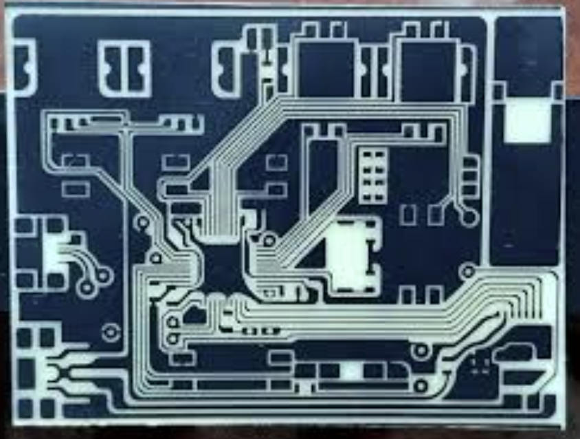
Next, the board goes into a chemical etch bath that may contain ferric chloride or alkaline persulfate as an etchant. The etchant eats away all the unprotected copper very uniformly. This wet-etch process produces very precise, smooth-edged traces as accurate as the film resolution allows. Typical photoresist etch can easily do 4 mil (0.10 mm) lines and spaces on 1 oz copper, a level hardly attainable by a home laser. After etching, the remaining resist is stripped off, leaving just the copper circuit.
Compared to a brute-force laser burn, photolithography has minimal undercut and very consistent line widths. It also works identically across large panels – no variation from one side of the board to another as long as the exposure is uniform. Finally, chemicals can etch completely through copper cladding (even >2 oz boards) without mechanical force. In DIY, residual mask or incomplete etching often causes shorts or open circuits; industry minimizes these problems with tight process control.
Advanced Multi-Layer Buildup and Controlled Impedance
Professional fabs can build multi-layer boards that are beyond DIY reach. After creating each inner layer as above, the layers are stacked with prepreg in between. On a heated, pressurised laminator, the stack is fused into one solid board. This “layer-up” process aligns all the circuits together, with perfectly flat inner layers. The result is a board with internal power/ground planes, buried networks, and plated-through vias connecting layers. Another pro advantage is impedance control. High-speed digital and RF circuits require traces of very precise width and dielectric separation. Manufacturers meet these specs by tightly controlling layer thickness and copper weight. For example, JLCPCB even provides an impedance calculator for engineers.
Rigorous Quality Control, Testing, and Certification Standards
After fabrication, professional boards undergo thorough inspection and testing. Optical and electrical checks are routine:
- Optical Inspection (AOI): Every layer and the final board are scanned by automated optical inspection. The machines compare the actual board image to the intended design (Gerber). Boards that fail AOI are discarded before assembly.
- Electrical Testing: Many fabs also perform a flying-probe or bed-of-nails electrical test to ensure no unexpected shorts/opens. And they may do a high-voltage “burn-in” to check insulation. This guarantees the board meets IPC standards.
- Plating and Finishes: Pro boards have plated-through holes, which strengthen vias and connect layers reliably. They also receive finish coatings and soldermask so that copper is protected and solderable. A DIY laser board usually has none of that, leaving copper bare and vulnerable.
When Professional Manufacturing Is the Better Choice
Scenarios Where Industrial Methods Deliver Clear Advantages

Professional PCB fabrication becomes compelling whenever your project demands go beyond “simple toy.” Some clear cases:
- Fine Pitch or High Density: If your design has very thin traces or small pads like 0.5 mm pitch components, RF traces with controlled impedance for photolithography are better. JLCPCB’s minimum drill is 0.3 mm, and the minimum trace is 0.1 mm.
- Multi-Layer Boards: Need 4+ copper layers, blind/buried vias, inner power planes, or flexible/rigid-flex boards? Only a factory can do that. If your design grows beyond one or two layers, the complexity of alignment and lamination alone mandates professional service.
- Special Materials: High-Tg FR4, metal-core for heat dissipation, Rogers for RF, and polyimide flex are required for special applications. Pro fabs handle speciality laminates. Home lasers are generally limited to whatever off-the-shelf copper-clad sheet you have.
In essence, if your design will later see multiple runs, it should contain many parts. DA IY laser is really only a stopgap for the earliest prototyping.

Frequently Asked Questions (FAQ)
Q: Can I use a laser cutter at home to make a PCB instead of chemicals?
A: Not fully. Hobby lasers usually only remove a resist/mask. You still need chemical etching to remove copper. True copper ablation needs industrial lasers, not DIY ones.
Q: What is the finest detail a DIY laser PCB can achieve?
A: About 0.2 mm (8 mil) traces in practice. Fine-pitch parts or 0.1 mm (4 mil) designs require professional PCB fabrication.
Q: How do I make holes (vias) in my laser-etched PCB?
A: Holes are drilled manually after etching and are not plated. Layer connections need wires or solder jumpers. Professional fabs drill and plate vias automatically.
Q: Is it safe to laser-etch PCBs at home?
A: Yes, if done carefully. Use proper laser goggles, strong ventilation, and avoid inhaling fumes or etchant vapours. Treat it like a real workshop tool, not a toy.
Q: When should I stop laser engraving and send my design to JLCPCB?
A: When the design gets complex, it needs fine traces, double layers, reliability, or more than a few boards. For most cases, ordering from JLCPCB is faster, cheaper, and far more reliable.
Keep Learning
How Beveled Edges Improve Reliability and Performance in Card Edge Connectors
Key Takeaways Beveled edges enable smooth insertion and protect gold fingers from wear in card edge connectors. Use 30° or 45° angles (45° is standard for most designs) with depth of 1/3 to 1/2 board thickness. They reduce insertion force, prevent plating damage, and improve long-term contact reliability. Proper beveling is critical for high-cycle applications like DDR modules and PCIe cards. Bevel edges came into my attention the first time a memory module that I designed scratched its own gold finge......
How to Prepare Perfect Gerber Files for Flawless PCB Production
Key Takeaways Use RS-274X format and consistent millimeter units for all files. Always include complete layers: Copper, Solder Mask, Silkscreen, Board Outline, and NC Drill. Check your Gerbers in a viewer before uploading to catch errors early. Follow DFM rules: proper annular rings, solder mask expansion, and trace spacing. Use clear file naming and detailed fabrication notes. After spending weeks working on the perfect board layout, the routing is clean, the DRC passes, and you hit “export.” Two day......
Technical Guidance: V-Cut Panelization Standards
For boards with regular rectangular shapes, V-cut (V-scoring) panelization is an efficient method. This process involves cutting V-shaped grooves of a specific depth on both sides of the panel along the board boundaries, leaving a thin web of material (typically about 1/3 of the board thickness) that allows easy manual separation after SMT assembly. After separation, minor thread-like fibers or rough edges may remain and can be lightly scraped off. Due to material expansion and cracking during depanel......
Technical Guidance: Character Design Specifications
To facilitate component assembly, future maintenance, and traceability of PCB manufacturing information (such as manufacturer, production date, batch number, etc.), various character markings are typically silk-screened onto the PCB. These include component designators, polarity marks, test point labels, company logos, and production traceability information. Traditional PCB character silk-screening uses the screen printing process, hence the term “silk-screen characters.” High-definition characters a......
Technical Guidance: Mouse Bite Panelization Guide
The conventional method of panelization uses V-grooves. However, for irregularly-shaped boards or special requirements (such as JLCPCB's economic SMT assembly), mouse bite panelization, which resembles postage stamps on an envelope, is required. PCBs panelized using this method are called "mouse bite panels" or "mouse bite connections". Mouse bite panelization can be referred to as "universal panelization." As long as there is a position to add mouse bites, boards of various shapes can be interconnect......
Smart PCB Array Design for Higher Yield and Lower Production Costs
Key Takeaways Smart PCB array design is a critical strategy for achieving higher manufacturing yield and significantly lower production costs. By optimizing panelization with proper board spacing, V-scoring, tab routing, and mouse bites, designers can dramatically improve material utilization by 20-30%, enhance production throughput, and simplify handling and depaneling while minimizing mechanical stress and defects. Effective use of fiducials and careful component clearance further ensures high-quali......