PCB Layers Explained : Building Better Boards Through Smart Stackup, Standards, and Design Practices
14 min
A PCB is a sandwich of copper and insulating sheets that are stacked together to form a circuit board. Each PCB layer has a specific purpose; for example, some carry signals (traces connecting components), while others serve as solid planes for power or ground. Think of PCB layers like the floors in a building, where each floor can have a different role. We can think of it as offices (signals) on one floor and storage (ground/power) on another. The number of layers varies by design complexity, from just one up to a dozen or more in advanced electronics. In this article, we will see how to place these layers in a stackup effectively. How to minimize the EMI and increase the signal integrity of the circuit. This is all about how the layout is performed and how the placement is done by the user.
Defining Layers in Single vs. Multilayer PCBs
The most basic one is single-layer PCBs. They possess copper on one side of the board and hence a low manufacturing cost. This is what makes them suitable for low-cost circuits such as LED drivers.
The standard is the use of double-layer PCBs. Both the top and bottom have coppe,r and this doubles your routing options. The two layers are connected through minute holes known as vias that allow the movement of signals between layers.
Multilayer PCB employs three or more layers of copper. They typically have internal power and ground planes that are placed between signal layers. High-tech devices, including smartphones, laptops, and medical equipment, often use multilayers with dense routing and very strict noise management required.
The Evolution from Simple to Complex Layer Configurations
Early electronics often got by with single- or double-layer boards. But as devices grew more complex and speeds increased, designers had to stack on more layers. Every extra layer gives more room to route connections without crossings. Optimal layer count depends on functional needs and manufacturability constraints. In practice, low-end products stick to 2 or 4 layers for cost-effectiveness. Mid-range designs typically use 6 layers, while cutting-edge high-speed systems commonly use 8 layers or more. 8-layer boards are “best for high-speed/high-density designs”, with multiple plane pairs providing excellent EMI suppression and power stability.
Planning an Effective PCB Layer Stackup
A stackup is the ordered arrangement of all copper and dielectric layers from top to bottom. Getting the stackup right before routing traces is crucial. Because we cannot select any random layer and draw a trace on it, in a 4, 6, or 8-layer PCB, not all layers are treated as signals; randomly selecting layers may lead to serious signal integrity issues. A smart layer stack ensures clear return paths for currents and controlled impedance for high-speed lines.
Arranging Signal, Power, and Ground Layers Strategically
Ground and Power Planes (Decoupling Pair): Place solid ground and power planes in the middle of the board stack. When adjacent, they behave like a built-in capacitor, providing excellent decoupling. This will also reduce the loop inductance and overall system noise, as energy can be transferred more easily. A continuous ground plane beneath the signal layers provides return currents with a short, low-inductance path. Try to avoid routing a high-speed trace over a split or cut in the plane unless necessary. If you must cross a gap, use stitching vias to bridge the return path.
Signal Layer Placement: Put your most critical signals on layers immediately adjacent to a reference plane. Always place a solid ground plane beneath signal traces to maintain signal integrity and reduce EMI. For example, on a 4-layer board, one might use:
- Top = signals
- Layer 2 = ground
- Layer 3 = power
- Bottom = signals
This way, each outer signal layer is closely coupled to a plane, maintaining stable impedance.
Common Stackup Patterns for 4, 6, and 8-Layer Boards
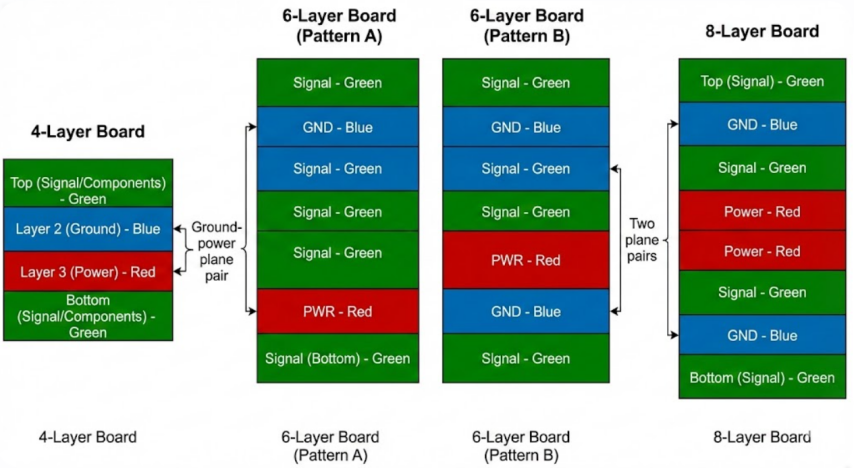
1) 4-layer Boards: So, a standard 4-layer stackup is typically Top (Signal/Components) - Layer 2 (Ground) - Layer 3 (Power) - Bottom (Signal/Components). I have seen them on many embedded projects and RF modules since they provide a reasonable tradeoff between routing density and impedance control and are not very costly.
2) 6-layer Boards: You can have plenty of room to play when you step up to six. Two configurations that I have purchased there are:
- Pattern A: Signal GND Signal Signal PWR Signal (bottom).
- Pattern B: Signal GND Signal PWR GND Signal.
Pattern A has an additional internal signal layer which contributes to de-congesting the routes. Pattern B leaves the power plane between two ground planes, so that is fantastic to blast the noise off. Pattern A I tend to use Pattern A when I require good power distribution, and Pattern B when noise immunity is the paramount consideration.
3) 8-layer boards: A typical layout resembles the following: Top (Signal) GND Signal Power Signal GND Bottom (Signal). What you end up with is a couple of power planes in the middle and ground planes on the 2 nd and 7 th layers. That is the gold rule of high speed designs, since the multiple plane pairs reduce loop areas and cut emissions.
Balancing Thickness and Material for Performance
Copper Thickness/Copper Weight: Thicker copper can carry more current and has a way of spreading heat, but it will also impact impedance. Wider or spaced copper wires are necessary to reach the same impedance as of smaller copper because of heavy copper traces. When creating a stackup, select copper weights that fit your requirements at this time.
Dielectric Thickness: The trace impedance is directly determined by the distance between a signal layer and a reference plane. As an example, a 5 mil (0.127 mm) trace on a 1.6 mm board with a Dk of approximately 4.2 has an approximation of 50 ohms when it is 0.2 mm away on the reference plane. Thinning the dielectric causes the impedance to decrease whereas increasing the dielectric thickness increases the impedance.
Board and Material Thickness: The typical PCB rigid boards are between 0.6 mm and 2.0 mm or more. A more bulky board is more effective in diffusing heat and a heat sink. Such a very thin board may be pliable, but it is more susceptible to warping or cracking in assembly.
Dielectric Material: FR-4 laminate is used as a standard board with Dk of approximately 4.3. In the case of RF or very high-speed signals, low-loss materials may be selected by the designer, e.g. Rogers material or PTFE based substrate which has lower Dk and dissipation factor to minimize signal loss. PCB material also has a role to play in setting stackup distances. Numerous impedance calculator (including the one on the JLCPCB) can assist you in choosing the appropriate thickness.
Adhering to PCB Layer Standards and Guidelines
Quality PCB design is not one that is just based on intuition, it must adhere to industry standards and best practices, and when critical layers are involved. The IPC (Institute for Printed Circuits) standard is the most common standard of consistency and reliability in PCB design:

- IPC-2221/2222 (Generic and Rigid Board Design): These constitute rules of general rules of trace widths, spacing, and layer stack optimization. They give equations to determine the lowest trace width that can be used with a particular current. The life expectancy of your traces after IPC-2221 is that they will not be overheated or arc, and your total layer stack will have sufficient dielectric spacing.
- IPC-2141 (High-Speed Design): This standard provides recommendations on signal integrity and impedance control in high speed boards. It explains how to create traces and layer stacks in order to reduce reflections and losses. IPC-2141 assists in maintaining your differential pair and single ended impedances on course.
- IPC-2152 (Thermal Management): Heat may destroy a board. IPC-2152 assists the designer in calculating the safe thickness with regards to traces and applies thermal reliefs in such a way that hot parts dissipate safely. It is useful to determine the design of copper planes and thermal vias.
Following these standards leads to the increase in reliability, simplified manufacturability, and compliance to regulations. Most PCB CAD packages, in practice, have IPC rule-checkers to assist in the enforcement of these guidelines during design.
Impedance Control and Layer Symmetry Requirements
1) Controlled Impedance: Every high-speed line typically targets a specific impedance here 50 Ω single-ended and 100 Ω for differential signals. That impedance is determined by layer geometry and the spacing of the dielectric between the trace and its reference plane. Use a fixed stackup, then adjust the trace width and spacing to hit the target. IPC and your PCB fab’s stack tables can guide these values. JLCPCB, for instance, provides impedance calculators that take your layer thickness and material into account to recommend trace widths.
2) Layer Symmetry: A well-controlled impedance board is usually symmetric around the center. This means dielectric thickness and copper distribution above the midplane mirror those below it. Symmetry prevents one side of the board from curing or expanding at a different rate than the other, which avoids bowing/warping. An unbalanced stack can “cause warping during manufacturing, leading to signal integrity issues”. To satisfy this, designers often specify a symmetric layer scheme in the PCB datasheet.
3) Signal Pair Routing: For differential pairs and other matched nets, keep them on a single layer and maintain equal trace lengths and spacing. This preserves impedance balance. Sierra Circuits recommends matching lengths to within a few mils and keeping diff pairs symmetrical to avoid skew. If a pair must cross layers, try to cross together via the same via hole.
High-Speed Design Rules for Layer Allocation
- Dedicated Reference Planes: Always give each high-speed net a clean return path. That usually means an uninterrupted ground plane directly beneath its layer. Without it, return currents might take a long detour through adjacent layers, causing noise and jitter. Place signals adjacent to their reference planes.
- Avoid Plane Splits: Do not route a fast signal over a gap between two planes. If a plane is split (one half is GND, the other PWR), a signal crossing that split has no local return path. If crossing is unavoidable, add stitching vias to tie the two halves of the plane together at that location.
- Separate Analog and Digital: In mixed-signal designs, allocate different layers and sometimes ground fills for analog and digital sections. This keeps noisy digital switching on its own plane, away from sensitive analog traces.
- Differential Pairs: Keep diff pairs on their own layers with fixed spacing. Ensure the layer stack provides the right differential impedance. If possible, route each pair on a layer adjacent to a solid ground plane to minimize loop inductance.
Advanced PCB Layer Design Techniques
Routing Strategies Across Multiple Layers
- Group Signals: Route-related or bus signals together on the same layer. For example, put all memory address lines on one layer and data lines on another. This keeps routings tidy and can simplify timing analysis.
- Minimize Via Use: Each via adds parasitic capacitance and inductance.
- Via Stitching: Place ground via “fences” or stitching around perimeters of sensitive areas and near connectors. This ties the planes together and provides local return paths for noisy currents.
Thermal and EMI Mitigation Through Layer Choices
Thermal Spreading: Copper is an excellent heat conductor. Internal copper planes naturally act as heat spreaders. More layers mean more copper to soak up heat. More layers help distribute heat, and internal copper planes act as spreaders. For a power-hungry design, dedicate an inner plane for thermal management and add thermal vias under hot components to tie them to that plane.
EMI Shielding: Solid planes serve as shields against radiation. Having multiple ground/power pairs reduces the loop area of signal currents. 8-layer boards, with their multiple plane pairs, achieve superior EMI performance by providing many return paths and confining radiated fields.
Common PCB Layer Troubleshooting and Fixes
Even with careful planning, issues can crop up. Here’s how to spot and fix common layer-related problems:
Identifying Signal Integrity Issues from Poor Stackup
Signals showing weird behavior often trace back to stackup problems. For instance, if a trace’s impedance suddenly changes due to an inconsistent dielectric, you’ll see reflections or bit errors on high-speed lines.
To diagnose:
- Look at your oscilloscope and TDR eye diagrams to see if they show unexpected reflections. That suggests impedance mismatches, often due to incorrect layer spacing.
- Check return paths and use a ground continuity check or simulation to ensure that, for each signal layer, the adjacent plane is indeed ground.
- Examine whether parallel traces on different layers are interfering; they may be sharing a poorly decoupled plane.
By correlating the symptoms with layer placement, you can often pinpoint a bad layer choice.
Resolving Crosstalk, Noise, and Warpage Problems

Crosstalk and Noise: This basically means that when signals are coupling with each other, some energies are shared between the two signals and this corrupts the signal and results in crosstalk. That is the typical workaround to either increase the distance between them or introduce a grounded layer. The other trick is to reassign one of the signals to a different layer which already has immediate ground reference. And also, but not least, add decoupling capacitors between the power and ground planes as close as possible to make your electrically connected with a wide frequency range. When the noise becomes extreme, it is possible to add some thin ground plane or guard traces between the noisy lines specifically.
Warpage: When the completed board is not straight or symmetrical, the most important is the stack symmetry. You will have to lay out the copper and prepreg again so that the two sides of the stack are identical to each other. As an example, the dielectric and copper over the midplane have to balance the same over the midplane as below. Apply the same number of cores that have copper cladding on either side. According to the industry rules, balanced stack essentially makes the majority of bowing issues non-existent.

Frequently Asked Questions (FAQ)
Q: Why do multilayer PCBs have so many layers?
A: More layers let you route complex circuits in a compact area and provide dedicated planes for power and grounding. Each extra layer gives more room for connections or a solid copper sheet for power/ground.
Q: What exactly is a PCB stackup?
A: The PCB stackup is the vertical order of all copper and insulating layers in the board. In simple terms, it’s how you “stack” the bread (copper) and filling (insulators) in your PCB sandwich.
Q: How does a ground plane work?
A: A ground plane is a solid sheet of copper that serves as the return path for currents and as an EMI shield. When placed directly under signal traces, it provides a short return path and helps maintain the characteristic impedance of those traces.
Q: What causes crosstalk, and how can I reduce it?
A: Crosstalk happens when two parallel signal traces couple energy between them. To reduce it, you can increase the spacing between aggressive lines or insert a grounded layer between them.
Q: Why is layer symmetry important, and what happens if my board is asymmetric?
A: Layer symmetry keeps the board balanced. If one side has more copper or thicker dielectric than the other, the board will likely warp or bend during fabrication and temperature changes.
Popular Articles
• PCBs Explained: A Simple Guide to Printed Circuit Boards
• Guide to the Top 10 Commonly Used Electronic Components
• Understanding the Basics of Electronic Devices and Circuits
• Choosing the Right Electronic Components for Your Electronic Design: Tips and Best Practices
• Digital 101: Fundamental Building Blocks of Digital Logic Design
Keep Learning
PCB Layers Explained : Building Better Boards Through Smart Stackup, Standards, and Design Practices
A PCB is a sandwich of copper and insulating sheets that are stacked together to form a circuit board. Each PCB layer has a specific purpose; for example, some carry signals (traces connecting components), while others serve as solid planes for power or ground. Think of PCB layers like the floors in a building, where each floor can have a different role. We can think of it as offices (signals) on one floor and storage (ground/power) on another. The number of layers varies by design complexity, from ju......
Integrating Standoff Spacers in PCB: Key Considerations for Mechanical Reliability and Performance
Standoff spacers are essentially small posts that serve as supports for circuit boards. They are much more than just small parts in a PCB assembly. These components work by lifting the PCB a bit, which then allows for proper airflow. So there will be better insulation and mechanical support. Standoffs keep a board steady and prevent it from touching other pieces. Choosing a good standoff can really change things; it ensures your device works right instead of failing or coming apart. With this, they ar......
PCB Holder Essentials: Top Types for Soldering and Circuit Board Stability Tips
A circuit board holder, also known as a PCB holder, is a mechanical fixture designed to clamp a PCB firmly in place. It secures the board so it won’t move during tricky operations like soldering, desoldering or testing. This hands-free support not only conveniences but also enhances safety and accuracy when you are working on delicate electronics. A good PCB holders ensure stability, keeping the board firmly located. Also helps in better alignment for positioning parts precisely throughout the assembl......
PCBs Explained: A Simple Guide to Printed Circuit Boards
Printed Circuit Boards (PCBs) are the essential building blocks behind almost all modern electronic devices. PCBs play an important role in that they provide electrical interconnections between electronic components, rigid support to hold components, and a compact package that can be integrated into an end product. They are the main component in an electronic device that is responsible for form and function, and they allow advanced semiconductors to communicate with each other at very high data rates.......
Guide to the Top 10 Commonly Used Electronic Components
Electronic components are fundamental elements of electronic technology serving as the essential building blocks of electronic circuits. As technology and its applications advance rapidly, the number of components used in design processes is increasing daily.It is crucial for electronic engineers or enthusiasts to master the characteristics and applications of commonly used electronic components. This article introduces the top ten electronic components commonly used by engineers and provides guidance......
Understanding the Basics of Electronic Devices and Circuits
In the realm of modern technology, electronic devices and circuits play a crucial role in powering everything from everyday gadgets to complex machinery. Understanding the fundamentals of these components can provide valuable insights into how various electronic systems operate and interact. This blog explores the basics of electronics devices and circuits, their types, functions, and the significance of their design in today's technological landscape. Electronics means the study of the flow of electr......