
How to Drag Solder Fine-Pitch ICs with Flux (Step-by-Step)
5 min
- Step-by-Step: How to Apply Solder Flux for Fine-Pitch & Drag Soldering
- Flux Tips for Fine-Pitch IC Drag Soldering
- Conclusion
Using flux correctly is critical for fine-pitch IC drag soldering. This guide covers key tips, common questions, and step-by-step techniques to prevent bridges and ensure strong, reliable joints.
Before getting into the step-by-step process, let’s answer the most common practical questions asked when using solder flux for fine-pitch IC drag soldering.
Q1: Why does Drag Soldering Require More Flux
Drag soldering relies on surface tension to snap the solder off the mask and onto the pins. Flux significantly reduces the surface tension of the solder, making it "want" to stick to the metallic pins rather than bridging across the non-metallic solder mask.
Q2: Flux Pen vs. Brush for Drag Soldering
A Brush or Gel Syringe is superior here. You need a generous, viscous layer of flux that stays in place while you drag the iron tip across multiple pins. A pen often applies a layer that is too thin and evaporates too quickly.
Q3: Where to Apply Flux for Fine-Pitch Leads - Pins Only or Pads Too?
Apply a continuous strip across the entire row of pads and pins. The goal is to create a "flux channel" that the soldering iron travels through.
Q4: How Much Flux Is Too Much for Drag Soldering?
While you need more than usual, flooding the entire chip body can cause the component to float or shift. Keep the flux confined to the pin rows.
Q5: Should You Reapply Flux Between Passes?
Yes. If you miss a bridge or need to re-drag a section, always add fresh flux. The old flux has likely exhausted its active ingredients and won't help separate the bridge.
Step-by-Step: How to Apply Solder Flux for Fine-Pitch & Drag Soldering
1. Component Alignment & Mechanical Anchoring: Carefully align the QFP/SOIC component leads with the PCB pads. Tack down two opposite corners (e.g., top-left and bottom-right) using a small amount of solder. This prevents the component from "floating" on the flux during the drag process.
2. Flux Channel Creation: Apply a continuous, generous bead of No-Clean Tacky Gel Flux across the entire row of pins. Unlike hand soldering, drag soldering requires a high-viscosity medium to act as a lubricant for the iron and a wetting agent for the solder. The flux should cover both the 'toe' of the lead and the pad extension.
3. Tip Selection & Loading: Use a Hoof or Bevel tip, which has a larger surface area and can hold a "reservoir" of molten solder. Load the tip with a small ball of solder - this reservoir will supply the joints as you move.
4. The Drag Technique: Place the soldering iron tip at the start of the pin row. Let the flux activate (fizzle). Drag the tip steadily across the pins at a medium pace. The flux reduces the surface tension of the molten solder, causing it to "snap" onto the heated metal leads while rejecting the solder mask between them.
5. Bridge Remediation: If solder bridges form between pins, do not panic. Apply fresh flux directly to the bridge. Clean your iron tip (remove excess solder), then touch the bridge again. The high activity of the fresh flux, combined with the clean tip, will wick the excess solder away, separating the pins.
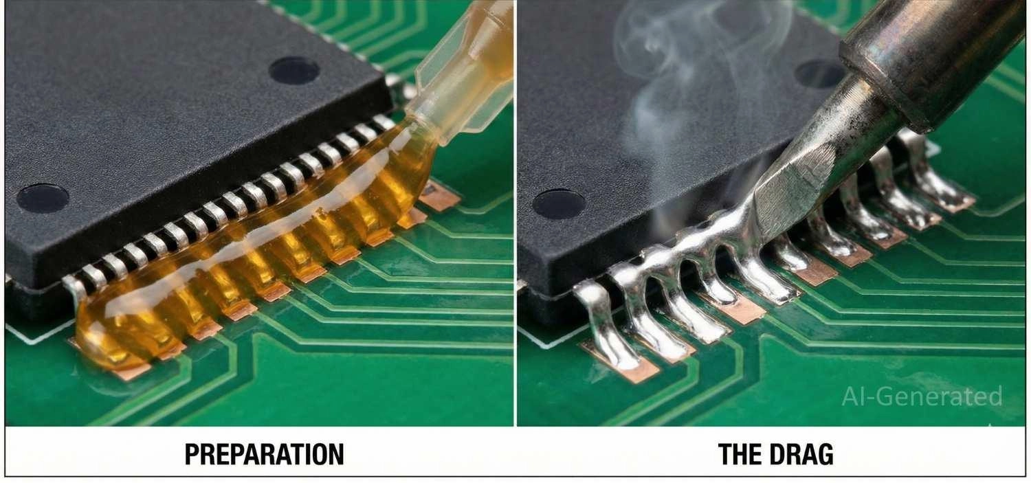
Figure: Applying a gel flux strip for drag soldering to prevent solder bridges on fine-pitch ICs.
Flux Tips for Fine-Pitch IC Drag Soldering
For experienced fine-pitch IC drag soldering, small flux practices can make a big difference in joint quality and repeatability.
1. Preheat the Board Slightly
● Warming the PCB slightly (40–50°C) helps flux activate faster and improves solder flow for very fine-pitch ICs.
● Avoid overheating, which can cause solder to ball or components to shift.
2. Minimize Oxidation During Pauses
● If you pause mid-drag, lightly touch the iron tip to a pad near the last joint to keep the flux active and prevent oxidation.
● This is especially useful for longer ICs or when working on lead-free solder.
3. Use Pin-to-Pad Capillary Action
● Angle the solder tip slightly along the pad to encourage solder wicking along the pin edges.
● This reduces the chance of cold joints without adding extra flux.
4. Limit Flux on Adjacent Components
● Mask or carefully avoid spreading flux onto nearby ICs or sensitive passive components.
● Excess flux may create bridging or unintended wetting during drag.
5. Control Humidity and Workspace Conditions
● Flux performance can degrade in very humid or very dry environments.
● Keep boards and flux containers sealed when not in use and work in a stable environment for consistent wetting.
6. Post-Solder Cleaning (Optional but Helpful)
● Even with no-clean flux, lightly brushing off residual flux with a soft brush or isopropyl alcohol can prevent long-term corrosion or residue on fine-pitch leads.
Conclusion
Proper use of solder flux is essential for reliable fine-pitch IC drag soldering. Applying flux correctly, maintaining active flux during the drag process, and controlling workspace conditions prevent bridges, cold joints, and component shifts. Even small practices—like preheating the PCB slightly, minimizing oxidation during pauses, and careful post-solder cleaning—can significantly improve joint quality and consistency.
Popular Articles
• Common PCB Assembly Methods and Soldering Techniques Explained
• What Is BGA Void? Causes, IPC Limits, and Solutions
• SMD Soldering Tools You Need: Complete Guide from Beginner to Pro
• Reflow Soldering: Everything You Need to Know
• SMT Assembly Process Explained and Equipment Used: A Step-by-Step Guide to PCBA Manufacturing
Keep Learning
12 Professional Soldering Tips and Tricks Every Beginner Should Know
Soldering is not merely "gluing" metal; it is a metallurgical process that creates an intermetallic compound (IMC). This molecular bond ensures the electrical and mechanical integrity of your device. A poor joint might pass a quick visual check but will inevitably fail under vibration or thermal stress, leading to "ghost" bugs and hardware failures. These soldering tips and tricks focus on practical, repeatable techniques used in professional electronics soldering—from correct heat transfer and flux u......
Solder Melting Point Guide: Chart, Alloy Types, and Reflow Considerations
In the precise world of electronics manufacturing, a difference of just a few degrees can mean the distinction between a perfect, reliable solder joint and a catastrophic "cold" joint failure. While many hobbyists view soldering simply as "melting metal to stick things together," professional PCB assembly requires a nuanced understanding of thermodynamics. The solder melting point is not simply a single value listed in a datasheet; it is a decisive limit that determines the choice of components, the s......
The Ultimate Guide to Solder Flux: Everything You Should Know Before Soldering PCB
Soldering is needed to make almost all electronic devices. Adding solder alone won't make a joint that is strong, clean, and sound from a metallurgical point of view. Solder flux is a very important part of the process that comes in here. If you want to do your job better and make it more reliable, you need to know a lot about soldering flux, whether you're an engineer, a professional technician, or just a hobbyist. This article goes into a lot of detail about solder flux, including what it is, how it......
Common PCB Assembly Methods and Soldering Techniques Explained
Whether you're designing your first prototype or scaling up to production, understanding PCB assembly methods and soldering techniques is crucial to achieving reliable, high-performance circuit boards. Modern PCBA primarily relies on Surface Mount Technology (SMT) and Through-Hole Technology (THT)—each offering unique advantages for component density, durability, and manufacturability. In this guide, we'll break down the major PCB assembly methods, key soldering techniques such as reflow and wave sold......
Flex PCB Assembly Guide: Process, Challenges, and Solutions
Flexible Printed Circuit Boards (Flex PCBs) are the foundational technology enabling the compact, innovative design of modern electronics. Because of their ability to bend and fold, they power devices from smart wearables to compact medical instruments where traditional rigid printed circuit boards (Rigid PCBs) can't be used. Achieving a functional electronic circuit from the raw plastic film demands special expertise, with flexible PCB assembly (FPCA) representing the crucial final step in this trans......
SMD Rework Guide: Tools, Temperatures, and Techniques That Prevent PCB Damage
From replacing a burned regulator to correcting wrong component values or removing solder bridges on fine-pitch ICs, SMD rework is an essential skill in electronics manufacturing and prototyping. It allows engineers to repair assembly defects, implement design changes, and recover valuable PCBs without the cost and delay of building new boards. In this guide, you will learn: What SMD rework is Common rework scenarios Tools and temperatures Safe removal and installation Package-specific techniques Real......