Inside the PCB Structure : How Layers, Stackup, and Buildup Define Modern Circuit Board Performance
14 min
Printed circuit boards may look like flat green rectangles, but beneath the surface, they are sophisticated multi-layer structures. As devices get more compact and complex, engineers turn to multilayer boards with carefully chosen materials and stackups to meet electrical and mechanical demands. This article peels back those layers to explore how substrate choice, layer stackup, and buildup methods shape PCB performance. Here we’ll cover PCB design fundamentals from the base materials up to high-density interconnects. Along the way, we’ll refer to industry guidance on best practices and cost trade-offs. I will show a comparison of different stackups that are often used and have become the industry standard over time.
The Core Elements That Form Any PCB Structure
Substrate Materials and Copper Foil Foundations
Every PCB starts with a substrate, which is like the insulating the backbone of the board. The most common is FR-4. FR-4 is inexpensive, mechanically strong, and has a moderate dielectric constant, which makes it a versatile all-purpose substrate. The problem is higher losses at RF frequencies due to the tangent and dielectric factor. That’s how the RF and microwave boards turn towards Rogers laminates. Because it comes with stable dielectric constants and ultra-low loss of around 0.001. Rogers is way better but costs roughly 5–10× as much as FR-4.
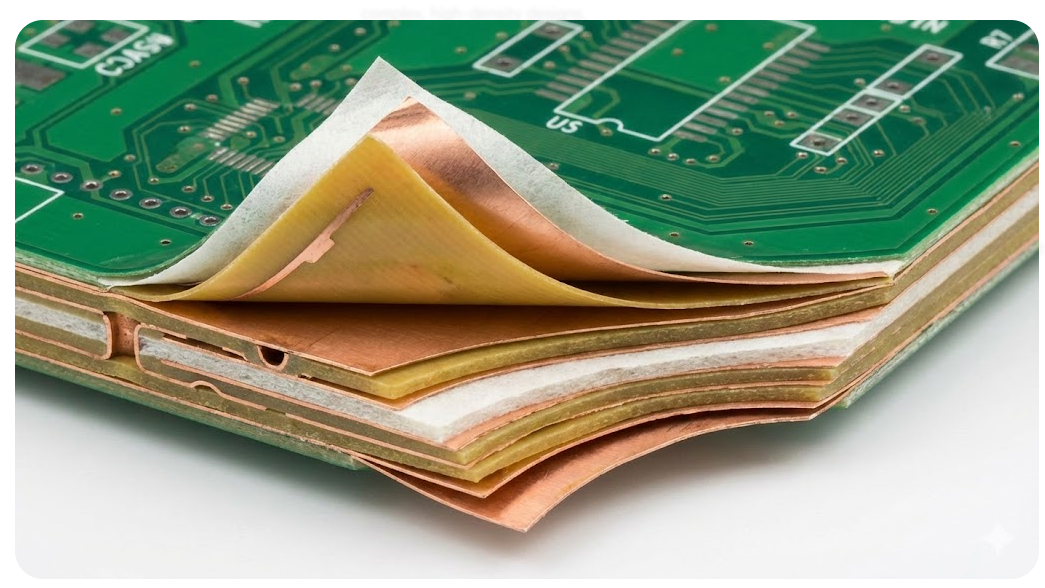
The next thing to put on a substrate is copper foil, which is laminated to it. The number of laminates defines the number of layers in a PCB. Typical copper weights range from 0.5 oz to 2 oz. This weight depends on the current carrying capability, and can be tuned as per that. We can use the thinner are lower weight to carry signals put power traces should be routed with a thicker copper.
Prepreg and Core Layers in Basic Buildup
A core is simply a pre-laminated piece of substrate with copper on both sides. It is a stiff, cured sheet that forms the board’s foundation. A standard 1.6 mm board might be built from one or more cores. During lamination, prepreg flows under heat and pressure to bond the cores together and bond copper foils on the outside. The final thickness of a prepreg layer depends on the applied pressure and resin content, so it can vary by ±10% after lamination. In practice, a multilayer board might use several core prepreg sandwiches. A common 6-layer stackup uses two cores with prepreg layers between them and on the outer faces.
Core vs. Prepreg (Side-by-Side): Core materials are rigid and precisely thickness-controlled, so designers often place critical inner signal & plane layers on cores for impedance stability. Prepreg is excellent at filling irregular gaps, but by itself it offers less impedance precision than a solid core. We can think of the core as the PCB’s skeleton and prepreg as its connective tissue.
Decoding PCB Layers and Their Functions
Signal Layers vs. Power/Ground Planes
Signal layers carry the routed traces and component pads. The power and ground planes serve very different roles: they act as stable voltage references and supply distribution networks. We can not run traces, signal, and power on all the layers in a PCB. In a typical multilayer board, designers will dedicate one or more inner layers to continuous copper planes. A ground plane provides a low-impedance return path and acts like an EMI shield. A power plane distributes, +3.3V or +5V across the board. And when placed adjacent to a ground plane, form a parallel-plate capacitance that help in decoupling the noise.
Putting power and ground close together is good practice and known as plane pairing. It will dampen the power-distribution noise and minimize loop inductance. Ground planes also reduce phenomena such as ground bounce and fast transient fluctuations. This is why designers place bypass capacitors right at IC supply pins and keep the local ground quiet by forming a tight local loop.
The Impact of Layer Count on Design Complexity
Each time you double up layers, you roughly double the routing capacity and the separation between planes. But at the same time, the cost and manufacturing difficulty of the board increase. At one extreme, a simple 2-layer board is cheap and straightforward, but routing can get cramped if there are many nets.
A 4-layer board typically adds one power plane and one ground plane inside. This lets you bury one plane between two outer signal layers. Designers often stack 4-layer boards as:
- Signal
- Ground
- Power
- Signal
You get superior decoupling and impedance control compared to 2 layers, so 4-layer is often the minimum for decent mixed-signal or RF designs. The downside is that the cost of adding those two extra laminated layers adds about 30–40% to the price.
With a 6-layer board, you gain two additional routing or plane layers. Common 6-layer arrangements are, for instance:
- Top (Signal)
- GND
- Signal
- Signal
- PWR
- Bottom (Signal)
This lets you put nearly every signal layer adjacent to a plane for controlled impedance and short returns. Another variant is
- Top
- GND
- Signal
- PWR
- GND
- Bottom
This will enhance noise immunity as a signal layer is sandwiched between power and ground. More cost and complexity leaps are to be expected here; 6-layer boards are sequentially laminated and have more vias, thus the tolerance of alignment narrows. In more complicated circuitry, we may graduate to an 8-10 or 12-layer board. The stackup information may be viewed in the JLCPCB material section. The number of layers is a design knob, and as the number of layers increases, we can control routing density and power distribution. The general rule of thumb is to have fewer layers where cost is a concern.
Inner vs. Outer Layers in Multilayer Boards
The outermost layers have some special roles compared to the inner ones. Outer layers host the surface-mounted components and connectors, so they carry all the footprints and dense routing needed to link parts. Inner layers, in contrast, cannot hold surface parts or exposed components; they often serve as internal signal routing layers or continuous plane layers.
Traces on an outer layer sit between copper on one side and air on the other, known as microstrip. At the same time, inner-layer traces are sandwiched between dielectric on both sides, known as a stripline. Inner layers, therefore have higher capacitance per trace and more shielding, which can lower impedance for a given trace width. This is why high-speed differential pairs are often buried so the signal sees ground planes immediately above and below. Designers typically put noisy or high-speed nets on inner layers between reference planes. JLCPCB recommends that, in a multilayer board, ground and power planes be placed as inner layers to act as shields. Meanwhile, outer layers still handle higher-voltage or IO connections where immediate plane adjacency is less critical.
Mastering PCB Stackup for Optimal Results
Standard Stackup Configurations (2‑Layer to 8‑Layer Examples)
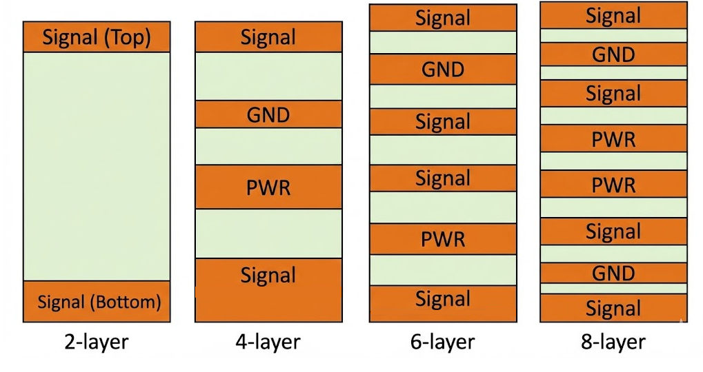
- 2-layer PCB: There is no inner plane; both top and bottom are signal layers. Often designers will pour one side as a ground or power plane to improve return paths. A typical 2-layer might route most nets on the top and use the bottom as a pseudo-ground pour for everything. This is cost-effective but limits how many nets you can run.
- 4-layer PCB: Here, the top and bottom are devoted to components and routing, while the inner two are solid planes (one ground, one power). For instance, L1=Signal, L2=GND, L3=VCC, L4=Signal. This yields excellent decoupling and allows tight control of trace impedance. Either way, 4-layer boards strike a balance of improved performance with moderate cost.
- 6-layer PCB: Top(Sig) – GND – Sig – Sig – PWR – Bottom(Sig). Note there are now three signal layers and two plane layers. In this example, two adjacent signal layers are sandwiched between ground and power to control impedance tightly and reduce crosstalk. An alternate 6-layer stack is Top – GND – Sig – PWR – GND – Bottom, giving even better noise immunity by having the power layer surrounded by grounds. In practice, choose a layout that balances your signal critical layers against how many planes you need.
- 8-layer PCB: An illustrative 8-layer stackup might be: Top(Sig) – GND – Sig – PWR – PWR – Sig – GND – Bottom(Sig). This gives two complete plane pairs, GND–PWR twice, and four signal layers. The advantage is maximal control, and you can put sensitive traces between planes on a signal layer with ground on each side, which yields superb return paths and EMI reduction. Of course, 8 layers means a thicker board and higher expense, and fabrication must be carefully controlled.
Symmetry and Balance Rules in Stackup Design
One golden rule in stackup is symmetry. A PCB stackup should be balanced top-to-bottom to prevent warping and stress. In practice, this means mirroring copper weight and layer order around the board’s mid-plane. A symmetric 6-layer might have the same copper thickness on L1 as L6, L2 as L5, and L3 as L4. Why? Because unequal copper distribution causes uneven expansion when heated, the board can “bow” or twist. If you have a ground plane on L2, try to have a plane of similar copper density on the corresponding “bottom” layer. If the top layer has many parts and pours (lots of copper), the bottom should, too, or else the board will not laminate flat.
Controlled Impedance and Signal Integrity Considerations
Finally, we tie the stackup to signal performance. Controlled impedance means designing each trace to have a specific impedance, usually 50Ω single-ended or 90Ω differential. The stackup directly sets this by changing trace width and spacing. Changing to a prepreg layer or moving the reference plane alters that value. After choosing the substrate material. designers typically use calculators or field solvers to adjust these parameters until the calculated impedance is right.
A well-planned stackup helps signal integrity. Fast digital edges need a tight return path. So, as a rule, route high-speed traces adjacent to a plane. JLCPCB’s HDI design guide advises placing ground under the signal and power just above that to create a stripline for minimal radiation. Pairing planes creates capacitance that damps power noise. These strategies reduce crosstalk and electromagnetic interference (EMI). In fact, having ground planes on inner layers reduces the loop area and minimizes any ground bounce effect for fast transitions.
PCB Buildup Types and Manufacturing Implications
Sequential Buildup for High-Density Interconnect (HDI)
When you need extreme component density and many vias, you enter the world of HDI PCBs. These often use sequential lamination; the board is built in stages rather than all at once. A few layers are laid and bonded first, then vias are drilled and plated, then more prepreg and copper are added on top in a second lamination. This allows inclusion of microvias connecting adjacent layers, as well as blind/buried vias.
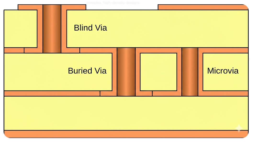
For example, A 12-layer HDI board might be made by first laminating 4 layers, then drilling holes to create buried vias. Then, stacking another 4 layers and drilling for buried vias, and finally, the last 4 layers. Prepreg sheets are inserted between each pair of subsets, and the complete lay-up is bonded together.
Foil vs Cap Buildup Methods Compared
PCB manufacturers use two broad approaches to layered construction: foil build and cap build. In a foil build, the outer layers are plain copper foil on a core, with prepreg between cores. A standard stackup is a foil build, first the outer copper foils, then layers of prepreg and cores, then inner copper. This is the most common method because it’s cost-effective and flexible.
A cap build, by contrast, uses cores on the outside. That means the very top and bottom layers are thick cores, not thin foil. Cap construction often uses no-flow prepreg on the outer faces so that the core thickness does not change. This approach is used when extreme material stability is needed, for example, in microwave or RF boards where the dielectric constant must not shift at all. By using cores on the outside, you eliminate one source of variation.
Below is a quick comparison table of these methods:
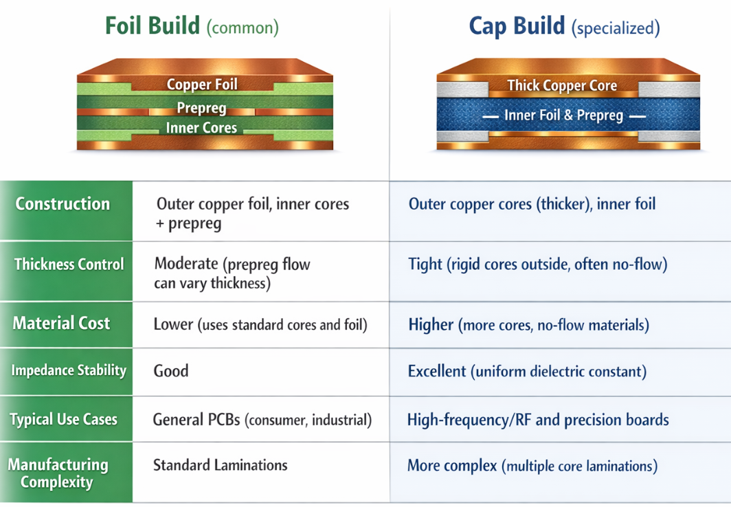
In short, foil builds are the go-to for most boards because they strike a balance of cost and performance. Cap builds are chosen only when needed for performance-critical signals. If a board uses both, it truly becomes a hybrid or mixed build, and the designer must work closely with the fab house to select materials.
Hybrid and Rigid-Flex Structure Variations
In addition to rigid PCBs only, there are cases when hybrid or rigid-flex structures are required by a designer. The hybrid PCB may be a blend of various materials in a single overall PCB, or it can imply a blend of multi-layers (rigid) and flex components. Rigid-flex PCB is literally constructed by bonding rigid layers to flexible ones.
Polyimide flex flex sections are built with thinner copper (usually 1 oz or less), and no-flow prepreg such that resin does not creep into the flex. Fine lines with drops are applied and the vias are not placed too close to the lines of the folds. Thermal behavior is also different because flex zones do not have a lot of copper to dissipate heat. Therefore, thermal generating components are often limited to the rigid segments where thermal vias or planes can be of assistance.
Physical Design Factors Influenced by Structure
Thermal Management and Mechanical Strength
The heat and mechanical behavior is highly dependent upon the layer structure of a PCB. Additional copper and layers tend to enhance the spread of heat. Largely, internal power/ground planes may serve as huge heat sinks, carrying heat off hot devices laterally. Nevertheless, this may turn out to be a two-sided sword since the greater the stiffness, the greater the thermal stress in case of temperature variations, and that is why symmetric stackups are essential to maintain the board flat. The rate of expansion of FR-4 and polyimide is not the same as that of copper, and thus, any mismatch may lead to peeling. In rigid-flex, the mitigation of these stresses is done by using no-flow prepregs and low-CTE materials.
Cost, Size, and Manufacturability Trade-Offs
Finally, let’s look at the practical trade-offs of choosing one structure over another. More layers generally increase cost. As one JLCPCB analysis notes, going from 4 to 6 layers or 6 to 8 layers typically bumps the price by 30–40% per step. Additional factors like heavier copper, exotic materials, or microvias also add expense. On the other hand, a higher-layer stackup often lets you shrink the board area for a given circuit, which can offset cost. Packing more into a smaller footprint saves PCB area, even if each board is pricier per sq cm.
JLCPCB’s free DFM feedback is very helpful at the design stage. It will scan your Gerber and flag common issues that fall out of these trade-offs. For instance, the DFM tool can catch if a trace is too thin for the intended copper, if spacing rules are violated, or if a plane is broken by an unintended gap. It even checks for thermal issues, e.g., it can warn if a heat-generating component lacks enough copper or vias for heat sinking.
Frequently Asked Questions (FAQ)
Q: What exactly is a PCB stackup?
A PCB stackup is the ordered arrangement of copper layers and dielectric (insulating) layers in a board. It defines how many layers there are and what each layer’s purpose is.
Q: How do I decide how many layers I need?
It depends on routing needs, signal integrity, and budget. A simple design might only need 2 layers, but high-pin-count or high-speed circuits usually benefit from 4+ layers to add dedicated power/ground planes and extra routing layers.
Q: What is the role of ground and power planes?
Ground and power planes act as reference sheets. A ground plane provides a low-inductance return path and EMI shielding.
Q: Can JLCPCB help me verify my stackup?
Yes! JLCPCB provides stackup templates and impedance calculators, and their free JLCDFM tool will automatically check your design.
Keep Learning
Understanding PCB Thermal Conductivity : Material Choices, Calculation Methods, and High-Performance Solutions
When it comes to compact electronics, the challenge is power consumption, and thermal issues arise due to that. A PCB can pass DRC checks, SI simulations, and even functional testing, yet it may fail miserably in the field due to poor heat management. PCB thermal conductivity is no longer optional for electronics designers; it has become the core consideration in modern designs. As the component sizes shrink, the thermal margins disappear. When designing a PCB with complexities and compact assembly, o......
Inside the PCB Structure : How Layers, Stackup, and Buildup Define Modern Circuit Board Performance
Printed circuit boards may look like flat green rectangles, but beneath the surface, they are sophisticated multi-layer structures. As devices get more compact and complex, engineers turn to multilayer boards with carefully chosen materials and stackups to meet electrical and mechanical demands. This article peels back those layers to explore how substrate choice, layer stackup, and buildup methods shape PCB performance. Here we’ll cover PCB design fundamentals from the base materials up to high-densi......
PCB Material Guide : Types, Selection, and Impact on Performance
If PCB materials could talk, FR-4 would probably say, "I run 80% of the electronics industry, and still nobody appreciates me." Rogers would boast, "I'm expensive because I'm special," while Polyimide would flex literally and say, "I bend, but I don't break." The purpose of this blog is to introduce you to the types of PCB substrates available to you and how those materials affect your PCB's performance, thermal stability, signal integrity, and overall longevity. The choice of PCB material will be bas......
Aluminum PCBs vs. Traditional FR4: A Comparative Analysis of Thermal Management
In the rapidly evolving world of electronics, thermal management plays a crucial role in ensuring the performance and reliability of printed circuit boards (PCBs). As electronic devices become more compact and powerful, effective heat dissipation becomes essential. In this article, we will conduct a comprehensive comparative analysis of two popular PCB substrate materials: aluminum and traditional FR4. We will explore their thermal management capabilities, advantages, considerations, and provide valua......
PCB Repair Reality Check : Why It’s a Last Resort and How Proper Design and Manufacturing Prevent Most Issues
Printed circuit boards are like the heart and nervous system of electronic devices. When they start to fail, you need to know why. Standard failure modes include component breakdown, trace damage, and environmental stress. ICs can burn out, and tiny solder joints may crack under heat. Overheating can literally burn out circuit sections. A dropped device or dent often produces visible cracks in components. It can even corrode copper traces, causing shorts. In today's post, we will explore when to do re......
PCB Copper Pour Basics
What is Copper Pour in PCB Design? Copper pour refers to the technique of filling unused areas of a PCB's copper layers with solid copper planes. These planes are connected to power or ground nets, creating a continuous conductive path. Copper pour is typically used in the power and ground planes, as well as in signal layers for specific purposes. Purpose and Benefits of Copper Pour: Copper pour is primarily used to fill unused areas on PCB copper layers with solid (or hatched) copper connected to pow......