Why a Strong PCB Ground Plane Is Key to Noise-Free Designs : From Basics to Optimization and Fixes
15 min
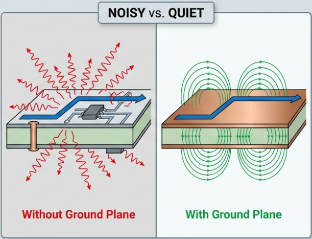
Every PCB designer eventually learns that the ground plane is like the unsung hero of the board. They quietly provide a reference point for all signals and a return path for currents. In essence, a ground plane is a large, continuous copper area tied to the 0V ground of the power supply. It spans most of an inner layer (or the entire layer) so that virtually every component lead or trace that needs ground can connect to it via a short via or pad. This creates a solid, low-impedance return path for signals, which helps reduce noise and electromagnetic interference by giving current pulses a wider range. In this article, we will see how to design a board effectively. If you just provide a better grounding to components, it will reduce the overall EMI and enhance the overall power integrity of the board.
What Exactly Is a Ground Plane and Its Primary Role
A ground plane can be thought of as a copper “sea” that ties together all ground nets. Unlike small ground traces, the plane’s large area holds many electrons, keeping the ground at virtually the same potential everywhere. This common reference plane means that switching currents (like those from digital ICs) don’t have to travel on skinny, long traces; they simply flow directly down to the nearest part of the plane.
A ground plane creates a solid, low-impedance return path for signals. This reduces EMI and minimizes ground loops and noise. The ground plane also acts as a shield of sorts, absorbing stray interference and clamping it to ground. A ground plane serves practical roles like thermal management and mechanical stability. The same copper that carries return currents can also spread heat away from hot components. Having large copper areas on the inner layers helps keep the board from warping under heat.
How It Differs from Power Planes and Vias
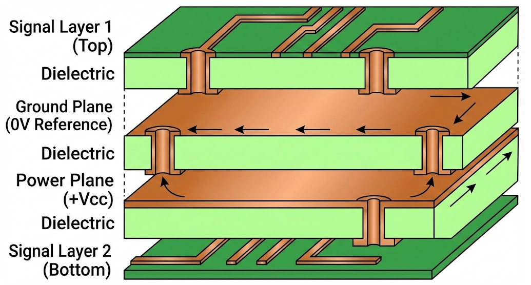
It’s easy to mix up ground planes with power planes, but they serve opposite (though complementary) roles. A power plane is a layer dedicated to carrying one of the supply voltages (like +5V or +3.3V) across the board, ensuring each component sees a steady source. In contrast, the ground plane is at 0V, the ultimate return for all currents. In a multilayer PCB, designers often put the power plane and ground plane on adjacent layers. This closely spaced “capacitor” of two copper sheets actually filters noise (a built-in decoupling effect). On a 2-layer board, there usually isn’t room for a full power plane, so the bottom layer is often used as a ground plane while power is fanned out with tracks.
Vias are the tiny copper-plated holes that stitch layers together, and they work hand-in-hand with planes. A Via can connect components or nets to the ground plane. In practice, a well-placed via is like a sturdy pillar supporting a roof. it ties the high-speed trace down to the ground plane below, so the return current has a direct path.
The Impact of Ground Planes on Circuit Board Performance
A properly implemented ground plane can dramatically boost PCB performance. Let’s break down the top benefits:
Reducing EMI and Crosstalk Through Proper Grounding
One of the biggest roles of a ground plane is noise reduction. By offering a low-impedance return path for all signals, the plane keeps loop areas small. Large loops act like antennas that radiate or pick up EMI, but a ground plane keeps the current loop close to the trace. This effectively shields sensitive traces from each other. When a high-speed trace has a solid ground plane right beneath it, the return current flows directly under the trace instead of looping all around. This confines the electromagnetic fields tightly and cuts crosstalk between adjacent lines. In fact, studies show that placing a ground plane in a stripline configuration can reduce crosstalk by tens of dB compared to a board without a ground plane.
Additionally, the ground plane acts like a Faraday cage for the board. It absorbs stray fields and noise, preventing them from disturbing circuits. If a nearby circuit tries to radiate interference, the ground plane soaks it up. The result is a much cleaner signal integrity. A solid ground plane provides a low-impedance path for return currents. In short, more ground plane means fewer spurious signals hopping between parts of the board.
Enhancing Signal Return Paths in High-Speed Circuits
High-speed digital and RF signals care a lot about their return paths, and the ground plane is critical here. A signal going up a trace must come down somewhere; without a nearby plane, its return path may take a long, indirect route through the board, increasing inductance and delay. When a ground plane is placed directly under a signal (like a microstrip or stripline), the return current follows directly under the signal path, creating a nice, controlled transmission line. This not only stabilizes impedance (e.g. 50Ω lines) but also minimizes delays and distortions.
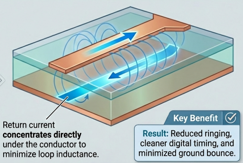
Instead, the return essentially shadows the forward path. The result is reduced ringing, faster edges with less overshoot, and lower radiation. When return loops are confined by a continuous plane, designers see much lower ground bounce and cleaner digital timing. In mixed analog/digital designs, an uninterrupted ground plane beneath high-speed digital traces prevents those currents from wandering into analog sections.
Benefits for Power Distribution and Thermal Stability
Although ground planes primarily serve signal integrity, they also aid power distribution indirectly. In a multilayer PCB, the proximity of a ground plane to a power plane forms a large, parasitic decoupling capacitor. This maintains a low-impedance power network, smoothing voltage and preventing sudden dips during switching. In simpler boards, having a robust ground plane means fewer voltage drops in the ground return, which keeps logic levels more consistent.
Moreover, the ground plane’s copper spreads heat. A solid ground pour acts like a heat sink: it draws heat from hot components and spreads it over a larger area, preventing local hotspots. Ground fills improve thermal performance and component lifespan. Power-hungry parts benefit from this passive cooling, and the board is less likely to warp or delaminate under heat. In short, even though it’s at “zero volts,” the ground plane provides voltage stability for signals and acts as a thermal cushion.
Best Practices for PCB Ground Plane Design
A ground plane only does its job if designed thoughtfully. Here are key best practices to keep your noise demons at bay:
Layer Placement and Split Plane Strategies
- Layer Stackup: Always use a balanced, symmetric layer stack to avoid board warpage. On multilayer boards, place ground planes on inner layers adjacent to signal layers. This maximizes coupling with signals and reduces EMI. For example, a common 4-layer stack is: Top (signals) – GND – PWR – Bottom (signals).
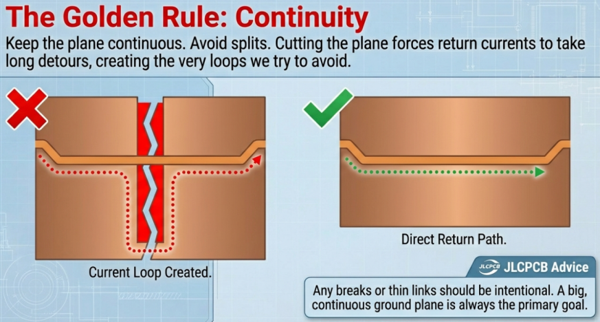
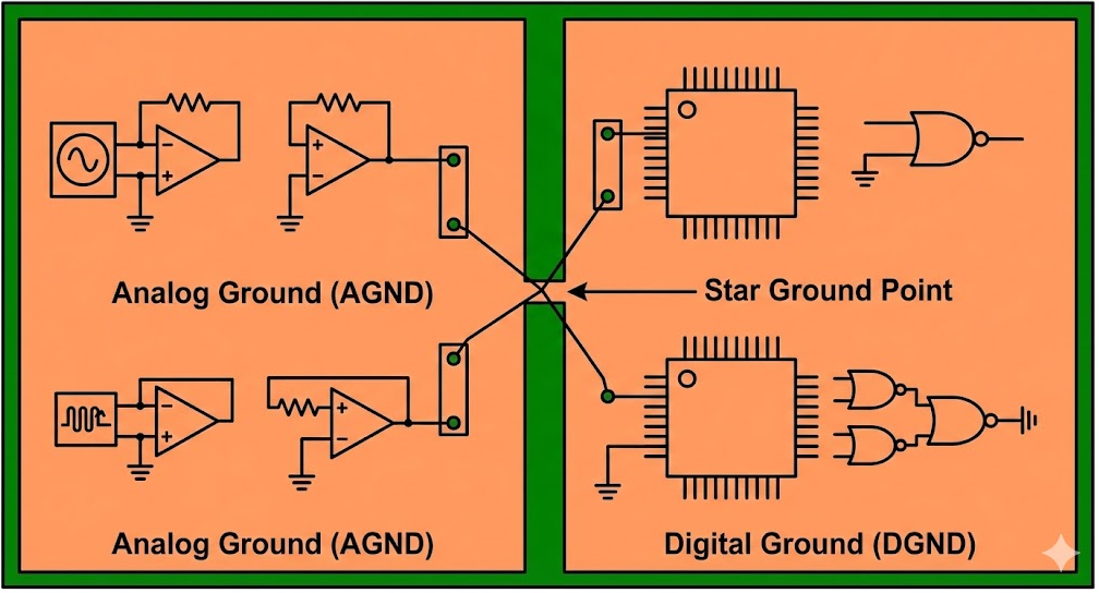
- Continuous vs. Split: Generally, keep the ground plane as continuous as possible. Avoid splitting the ground layer unless absolutely needed for separate analog/digital zones. If you must split grounds (say, analog vs. digital), make sure to reconnect them at a single star ground point. This ensures both sections share a reference without forming loops. JLCPCB advises separating analog and digital grounds to minimize coupling, but only if you stitch them together at one point to avoid floating potentials.
- Coverage: Dedicate as much area as possible to the ground plane. If your board is small or 2-layer, use copper pour (ground fill) on the unused spaces to extend the ground. The more complete the plane, the lower its impedance. Keep clearances of at least ~0.5 mm from signal traces when pouring (so you don’t accidentally short them) but flood the rest.
Via Stitching and Ground Fill Techniques
- Via Stitching: For split or large ground pours, use plenty of vias to stitch ground together. Multiple vias reduce inductance and create a robust connection across layers. Place via arrays around the perimeters and in large empty sections of the plane. This also turns the plane into a better shield. Cadence’s best practices specifically note that via stitching along plane edges improves shielding and reduces EMI.
- Ground Fill (Copper Pour): When you copper-fill unused areas, make sure to tie the fill to ground nets. Set your CAD tool to “thermals” or use small spokes to prevent isolation of pads. A solid pour increases current capacity and stability, while a hatched (grid) pour can save weight at high frequency. In high-speed designs, solid pours are usually best, but on 2-layer boards a hatched pour can ease manufacturing. The key is continuity: pour must connect to ground at regular intervals so no islands form.
- Thermal Reliefs: On dense copper pours, ensure thermal-relief spokes on pads, or soldering will be difficult. This is more of a manufacturing note, but a well-poured plane with proper thermal relief still does the electrical job.
Sizing and Thickness Considerations for Effectiveness
- Copper Thickness: Most PCBs use 1 oz copper (~35 μm thick) per layer. The ground plane thickness is the same as other internal copper. If you have very high currents on ground (rare except in power boards), you might specify 2 oz copper for inner layers to reduce resistance. In practice, 1 oz is enough for almost all signal return needs.
- Plane Sizing: The ground plane should cover as much board area as possible. Keep a solid pour on inner layers rather than hatched patterns, unless thermal stress is a concern. Inner solid planes give the lowest impedance.
- Divide with Purpose: If you have multiple ground domains (for example, digital, analog, chassis ground), think carefully before drilling them into separate islands. Unconnected “floating” ground islands will cause trouble. Instead, each domain should get its own plane or pour area, then all connected together at a single node (often at the power supply or a designated star point).
In short, a big, continuous ground plane is the goal. Any breaks or thin links should be intentional (for splitting noisy domains) and carefully managed. Follow manufacturer guidelines (like JLCPCB’s stackup recommendations) to ensure symmetry and manufacturability.
PCB Ground Plane Optimization for Advanced Applications
Balancing Impedance and Minimizing Loops
For controlled-impedance traces (50Ω lines, for instance), the ground plane is the other half of the transmission line. Consistent spacing between the signal trace and plane is crucial. In microstrip lines (trace on outer layer, plane one below), the designer must keep trace width and layer thickness fixed so impedance stays at the target. Similarly, for striplines (inner-layer trace flanked by ground on both sides), the idea is the same. If impedance mismatches occur, signals reflect and scatter – not good for GHz signals.
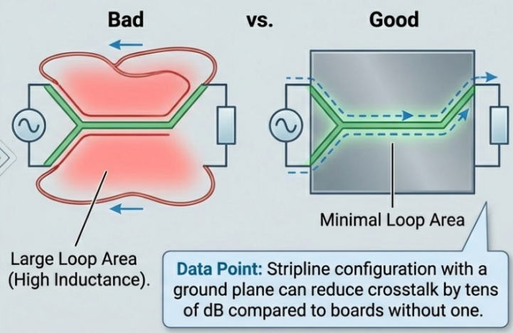
Loop minimization is equally vital. In RF and high-speed digital boards, every time a signal changes state, the return current jumps. A big loop area creates inductance; a small loop does not. By placing components and their bypass capacitors close to the ground plane, and ensuring the return path is short (preferably right beneath the signal path), we shrink those loops. The RF PCB guidelines from JLCPCB emphasize a “solid ground strategy” – with RF traces on the top layer and an uninterrupted ground plane just beneath. This direct coupling is the best way to keep loops tiny.
Tools and Simulations for Optimal Layout
Modern PCB CAD tools make designing and verifying ground planes easier. Tools like OrCAD, Altium, and KiCad let you define fill areas and automatically repour copper when routing is done. They can also highlight unconnected copper that needs vias. Many packages now offer field solvers and EMI/PI simulators. You can simulate return paths and loop inductances, or check the impedance of your stackup. Don’t forget measurement tools: a real PCB layout can be probed with near-field probes and oscilloscopes to find unexpected noise hot spots. Simulation helps catch things like slot resonance in the plane or insufficient stitching.
Case Studies in RF and Mixed-Signal Boards
Consider an RF Wi-Fi board: Designers will almost always reserve a complete ground plane beneath the RF front-end. Use a continuous ground plane directly beneath RF traces and avoid any interruptions. In practice, that means your antenna feed line on the top layer sits above a full copper ground on the layer below. Any break in that plane would ruin matching and increase EMI. Furthermore, in mixed RF/digital boards, the RF and digital grounds might be kept separate on the plane but tied at one bridge point to prevent loops.
In a mixed-signal ADC board, analog circuits need their own clean ground, but they cannot float apart from the digital ground forever. The recommended tactic is to pour separate analog and digital regions on the ground plane and connect them with a short, low-impedance link near the power source. The takeaway is that advanced boards often partition the ground plane, but only under tight control and always with the overall return path in mind.
Tackling Common Ground Plane Problems and Solutions
Ground Loops, Noise Coupling, and How to Diagnose
A ground loop happens when there are multiple return paths between two points, causing a loop of current that can pick up stray magnetic flux. The cure is a solid star-ground approach: ensure each ground domain ties back to one common node. Noise coupling can sneak in when digital chips switch and dump surge currents into the ground.
The symptoms might be random glitches or analog shifts. To diagnose these, use an oscilloscope with a good ground spring or a spectrum analyzer. Focus on the power and digital chips; even cheap oscilloscopes can catch excessive ground bounce or AC ripple. Looking at decoupling capacitor voltages can reveal if return currents are misbehaving. In design, you can also simulate worst-case current spikes to see which part of the ground plane will be stressed.
Fixes for Split Planes and Improper Stitching
If your ground plane is split poorly or has floating islands, you’ll get weird ground-potential pockets. The fix is to stitch and reconnect. Your CAD tool will show unconnected nets, or you can eyeball gaps in the plane. Add vias to tie those areas to the main ground. For analog/digital splits, add a “hat” of copper or a short bridge at a single point. Splitting a plane can be done as long as the two sides are connected by a thin trace or connection of low impedance.
In general, more stitching is almost never a bad thing. If EMI or crosstalk crops up, pepper the border of your ground pour with via stitching. If you see little antennas (trace stubs or long returns), re-route them to go over the plane.
When to Use Isolated vs Solid Ground Planes

As a rule of thumb, use a solid ground plane whenever possible; it’s usually the simplest and lowest-noise approach. Isolated or split planes are special cases. You might isolate grounds for analog vs. digital, or high-speed vs. low-speed, but only if your board really needs it. If you do split, follow best practices, keep them on the same copper layer, and tie them together at one point. Fully separating grounds without a careful plan can cause undefined return paths.
One scenario for an “isolated” ground region is a high-voltage or noisy section that you want to prevent from affecting the rest. For most logic and RF circuits, however, a unified plane is best. The separation question often comes up in FAQs: Should I split my ground plane? Generally, the answer is no, unless you’re very confident in your return path analysis or following analog/digital partition rules.

Frequently Asked Questions (FAQ)
What is a ground plane in a PCB?
A ground plane is a large copper area tied to the circuit’s 0V reference. It acts as a common reference node for all signals and provides a return path for currents.
Why is a strong ground plane important for noise reduction?
A solid ground plane minimizes loop areas and offers a short, low-inductance return path. This dramatically reduces EMI and crosstalk between traces.
Can I skip a ground plane and just use ground fills on one layer?
On simple 2-layer boards, you can use a bottom copper pour as a ground, but it essentially becomes a ground plane. Routed ground traces have much higher impedance than a pour.
When should I use via stitching on a ground plane?
Via stitching is useful along plane edges, around high-speed traces, and near splits. Use it whenever you want to lower plane impedance and improve shielding.
As JLCPCB engineers note, a solid ground plane is one of the most effective tools designers have for clean signals and robust power distribution.
Popular Articles
Keep Learning
Keeping Your PCBs Cool : Practical Heatsink Strategies for Better Thermal Performance
The current PCBs are becoming insane, and hence the cooling of PCBs is absolutely necessary. Large power components such as CPUs, GPUs, SOCs, voltage regulators, and LED drivers all ooze heat as a side-effect of their operation. Therefore, as an example, it is common to have CPUs, GPUs, or SOCs with their own heatsink, or boards that are extremely dense or contain power items such as motors, power transistors, amplifiers, regulators, etc., can end up in hot spots. A small PCB may become hot whena lot ......
Why a Strong PCB Ground Plane Is Key to Noise-Free Designs : From Basics to Optimization and Fixes
Every PCB designer eventually learns that the ground plane is like the unsung hero of the board. They quietly provide a reference point for all signals and a return path for currents. In essence, a ground plane is a large, continuous copper area tied to the 0V ground of the power supply. It spans most of an inner layer (or the entire layer) so that virtually every component lead or trace that needs ground can connect to it via a short via or pad. This creates a solid, low-impedance return path for sig......
Amplifier PCB Design: Building Nosie-free Hi-Fi Boards
Designing a high-fidelity audio amplifier PCB requires balancing physics principles with modern techniques.We must maintain a pure signal and ensure the board is manufacturable. An audio amplifier circuit should start with a clean power supply and proper filtering. Use a low-noise input stage with correct biasing and an input coupling capacitor. We will see some design techniques on how to include bypass and decoupling capacitors. Ensuring proper grounding to reduce hum. Adding stability networks, suc......
PCB Impedance Control: Ensuring Signal Integrity in High-Frequency Circuits
Impedance measures the opposition of an electric circuit when alternating current is applied to it. It is the combination of the capacitance and the induction of an electric circuit at high frequency. Impedance is measured in Ohms, similar to resistance. If the impedances are different, reflections and attenuation occur that deteriorate the signal. For high-frequency analog or digital circuits, it is essential to protect the signals that propagate on the PCB from being damaged. In fact, signals above ......
Understanding Impedance Matching for High-Speed PCB Designs
With the advancement of technology and the ever wider application of integrated circuits, the frequency and speed of electronic signal transmission have been increasing, making it essential for PCB conductors to provide high-performance transmission lines. These transmission lines are responsible for delivering signals from a source to the input of a receiver accurately and completely. This requirement emphasizes the need for impedance matching. Electrical impedance, commonly represented as Z and meas......
Signal Integrity in High-Speed Rigid PCB Designs
We use the term signal integrity a lot, what actually is it? Is it something related to signal parameters or system parameters? In easy words when a signal travels through a piece of wire or transmission line some parameter gets changed from where it is transmitted and where it received. In case of high speed signals the signal loss is even more, which rises to the problem of data losing and signal corrupting. So what type of signal is getting disturbed and how is it getting changed? We have discussed......