
Mini Drone PCB Case Study: How JLCPCB Solved High-Density SMT and Double-Sided PCBA Challenges
13 min
- Project Overview: The Mini PCB Flight Controller
- The Challenges: High-Density & High-Speed PCB
- The JLCPCB Solution: A Unified PCB Assembly & In-Stock Parts Ecosystem
- From DFM to PCBA: A Technical Deep-Dive into the SMT Assembly Process
- Results & Outcome: A Fully Operational Flight Controller
- Customer Feedback
- FAQ about Mini Drone PCB
- Conclusion: High-Density SMT for Mini Drone PCB
In the rapidly advancing field of unmanned aerial vehicles (UAVs), the engineering challenge has shifted. The market no longer demands just smaller and lighter drones; it demands smaller, lighter, and smarter systems. This establishes an important engineering paradox - how do you put cutting-edge capabilities such as AI-driven flight, high-definition video, and adequate data logging onto a PCB that must be small enough to meet weight and cost limits?
This case study overviews how one embedded systems developer who specializes in IoT and electronics design approached this exact question. The objective was to design and manufacture a single, sophisticated flight controller on a mini 10x10cm PCB.
To make the project feasible, the design was constrained to a 2-layer board custom-shaped as the drone's frame, the result being optimal weight and cost. This challenging constraint necessitated a delicate balance between extreme functional density, which required a complex double-sided SMT assembly process, and the intricate physics of high-speed signal routing.
The project's success depended not only on a good design but also on a manufacturing strategy that could mitigate risks associated with the Printed Circuit Board Assembly (PCBA) and the procurement of its intricate Surface-Mount Device (SMD) components.
Project Overview: The Mini PCB Flight Controller
The core of the project was a single PCB designed to be the "all-in-one" brain and power system for a compact quadcopter. The component selection was ambitious as it consisted of a strong microcontroller and a complete set of SMD sensors and peripherals:
- Central Processor (MCU): The Espressif ESP32-S3 N16R2. This module was selected for its powerful dual-core processor, integrated 2.4 GHz Wi-Fi and Bluetooth 5 (LE), and native USB OTG support, which made it a great fit as a hub for all computation, communication, and on-the-edge AI processing.
- Imaging: The OV2640 camera module, connected via a 24-pin FPC connector, was chosen for its cost-effectiveness and good imaging capabilities. This module is crucial for First-Person View (FPV) flight and future computer vision applications.
- Stabilization: An MPU-6050 Gyro/Accelerometer (IMU). This 6-axis sensor provides the critical orientation and stability feedback necessary for controlled flight.
- Data Logging: A high-speed SD-MMC interface (via TF-Push peripheral). A crucial feature for logging high-bandwidth flight data and captured images locally, which is a significant step up from slower SPI-based SD card solutions.
The Challenges: High-Density & High-Speed PCB
A 2-layer PCB is the standard for simple projects, but it becomes an extreme engineering challenge when dealing with high-speed, high-density designs. The developer faced three primary technical hurdles.
1Extreme Component Density & 2-Sided Surface Mount Technology (SMT)
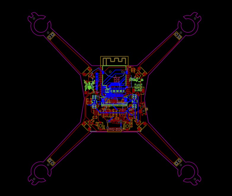
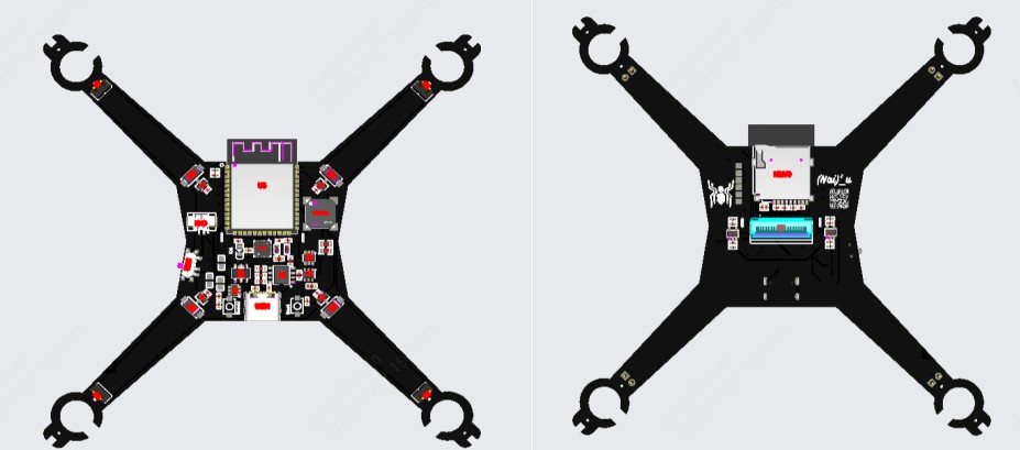
The 100x100mm maximum dimension was not a simple square; the board was milled into a complex "drone-frame" shape with motor-mount cutouts. This drastically reduced the usable surface area, amplifying the density challenge. To fit all functionality, a double-sided PCB assembly process was required, placing components on both the top and bottom.
- The top side incorporated the core compute elements (ESP32, IMU) and the entire power management subsystem (charging IC, regulators, etc.).
- The bottom side was packed with high-speed connectors (Camera, SD Card).
This high-density, double-sided SMT method on a complex-shaped board incorporated more than 70 SMD components from 31 distinct lines. Professional SMT assembly was essential due to fine-pitch packages (QFN, SOT-23-6) and a high volume of 0402 passive SMDs.
2High-Speed Signal Routing on 2-Layer PCB
The routing of many high-speed interfaces was the most significant technical barrier to overcome for the project.
- Parallel Bus Routing: The SD-MMC (4-bit) and OV2640 camera (8-bit parallel DVP) interfaces do not consist of simple serial buses. They operate as high-speed parallel buses with clocks that are extremely sensitive to signal skew (trace length mismatch) and noise.
- Routing Density and Crosstalk: On a 2-layer board, these sensitive signal traces must additionally route in proximity to each other and, most importantly, high-current motor traces and switching power supply lines. This presents a very high potential for noise injection and crosstalk that can quickly corrupt data, create artifacts on the camera, or cause the SD card to fail.
3Power Distribution
The PCB was designed to function as a sophisticated Power Distribution Board (PDB). Its role involved directing power from the LiPo battery, through protection ICs, to the charger, and subsequently to three independent low-noise voltage regulators.
The circuit board carried high-current pulses from the motor-control MOSFETs to the 8520 coreless motors. A courtesy of the 2-layer circuit board was the potential induction of high-current traces into neighboring sensitive analog power rails, which provide power to the camera and MCU, leading to instability in the final PCBA.
The JLCPCB Solution: A Unified PCB Assembly & In-Stock Parts Ecosystem
To mitigate risks in the manufacturing process, the developer transitioned from a traditional fab-only production model to a fully integrated PCB fabrication and assembly ecosystem.
JLCPCB's combined PCB manufacturing and double-sided SMT assembly services were selected to address these challenges.
The main concern—achieving reliable soldering of fine-pitch SMD components on both sides of the board—was quickly resolved using JLCPCB's advanced PCB assembly service.
A key enabler of this project was the JLCPCB In-Stock Parts Library, which proved critical to the design and production workflow. The engineer designed the board entirely around SMD components verified as in-stock in JLCPCB's database, referencing their exact part numbers. This decision fundamentally simplified the project's logistics and ensured supply continuity.
Notably, the library included not only the ESP32-S3 module, but also the entire SMT-based bill of materials (BOM). The developer sourced all 31 distinct SMD components—from the ESP32-S3 to the 0402 resistors—from JLCPCB's centralized inventory. This integrated approach ensured BOM compatibility, part availability, and streamlined PCB assembly from a single supplier.
From DFM to PCBA: A Technical Deep-Dive into the SMT Assembly Process
This project serves as a modern "DFM-first" (Design for Manufacturability) workflow, which is crucial for achieving successful PCBA outcomes.
-
Design for Manufacturability (DFM) with the Parts Library
The design process was highly iterative. Instead of completing the schematic first and then searching for components, the developer worked with the JLCPCB Parts Library open alongside the EDA software throughout the design phase.
Each essential SMD component — from the 3.3V LDO regulator to the battery protection IC — was selected directly from the JLCPCB library. Only In-Stock parts were chosen, and their exact part numbers and footprints were inserted into the schematic.
This proactive approach ensured that the Bill of Materials (BOM) and Component Placement List (CPL) were fully compatible with JLCPCB's SMT assembly line even before routing began. As a result, the developer effectively avoided common "part not found" errors and sourcing delays that often hinder rapid PCBA prototyping.
-
Board Specifications & High-Speed PCB Layout
The final 2-layer board design relied on JLCPCB's manufacturing precision to realize the difficult high-speed routing.
Parameter Specification Purpose / Challenge Board Size 100mm x 100mm Compact drone frame Layers 2-Layers Cost/weight optimized; high-speed routing challenge Material FR-4 Standard, reliable, strong High-Speed Routing Yes (Parallel Buses) Critical for SD-MMC/Camera on 2-layer; routing density Surface Finish ENIG (Electroless Nickel Immersion Gold) Flatness for fine-pitch SMD parts SMT Service JLCPCB SMT Service Double-Sided (2-Sided) SMT placement of all 70+ SMD components The decision to use an ENIG surface finish was intentional. For circuit boards that include fine-pitch surface-mount device (SMD) packages such as quad flat no-leads (QFNs), electroless nickel immersion gold (ENIG) offers a completely flat, lead-free surface.
It is a superior choice to hot air solder leveling (HASL) because it minimizes solder bridging and ensures reliable solder joints on every pad of leadless components during the surface-mount technology (SMT) reflow process.
-
Key Components Sourced & Assembled by JLCPCB
The "drone-on-a-chip" system, including its full Surface-Mount Technology (SMT) bill of materials, was entirely sourced and assembled at JLCPCB due to the extensive parts library.
The diverse categories of unique Surface-Mount Device (SMD) components used are summarized in the table below.
Component Category Key Parts Sourced & Assembled Package Types Microcontroller ESP32-S3-WROOM-1-N16R2 QFN Sensors MPU-6050 QFN-24 Power Management TP4056, DW01A, FS8205A ESOP-8, SOT-23-6 Voltage Regulators XC6220B331PR-G, ME6211C28, ME6211C15 SOT-89-5, SOT-23-5 Motor Control SI2302A-TP (x4) SOT-23-3 Connectors TYPE-C 16PIN, ZX-0.5 FPC-24P, TF-PUSH Card Slot SMT Passives 10k, 1k, 100k, 5.1k, 1.2k, 100Ω Resistors 0402, 0603, 0805 Capacitors 10uF, 100nF, 2.2nF Capacitors 0805, 0402, 0603 Other Peripherals SMT Switches, SMT LEDs, SMT Buzzer SMT -
Automated Assembly of Fine-Pitch & SOT Components
With a design featuring all unique SMT components (totaling over 70 individual SMD placements), including two QFN packages, multiple SOT-23-6 ICs, and dozens of 0402 SMD passives, manual assembly was not a viable option.
This challenge was amplified by the double-sided SMT assembly requirement, which involves two separate, high-precision solder paste, placement, and reflow cycles - one for each side of the board.
JLCPCB's automated PCB assembly service, which utilizes high-speed SMT (Surface-Mount Technology) lines, was essential for this complexity. This process includes the precise solder paste stencil, high-speed Pick-and-Place (PNP) for all SMDs, and multi-zone reflow ovens, all performed for both sides of the board.
This PCB assembly service mitigated the risk of SMT assembly failure, leaving only four simple through-hole headers for the developer to solder manually.
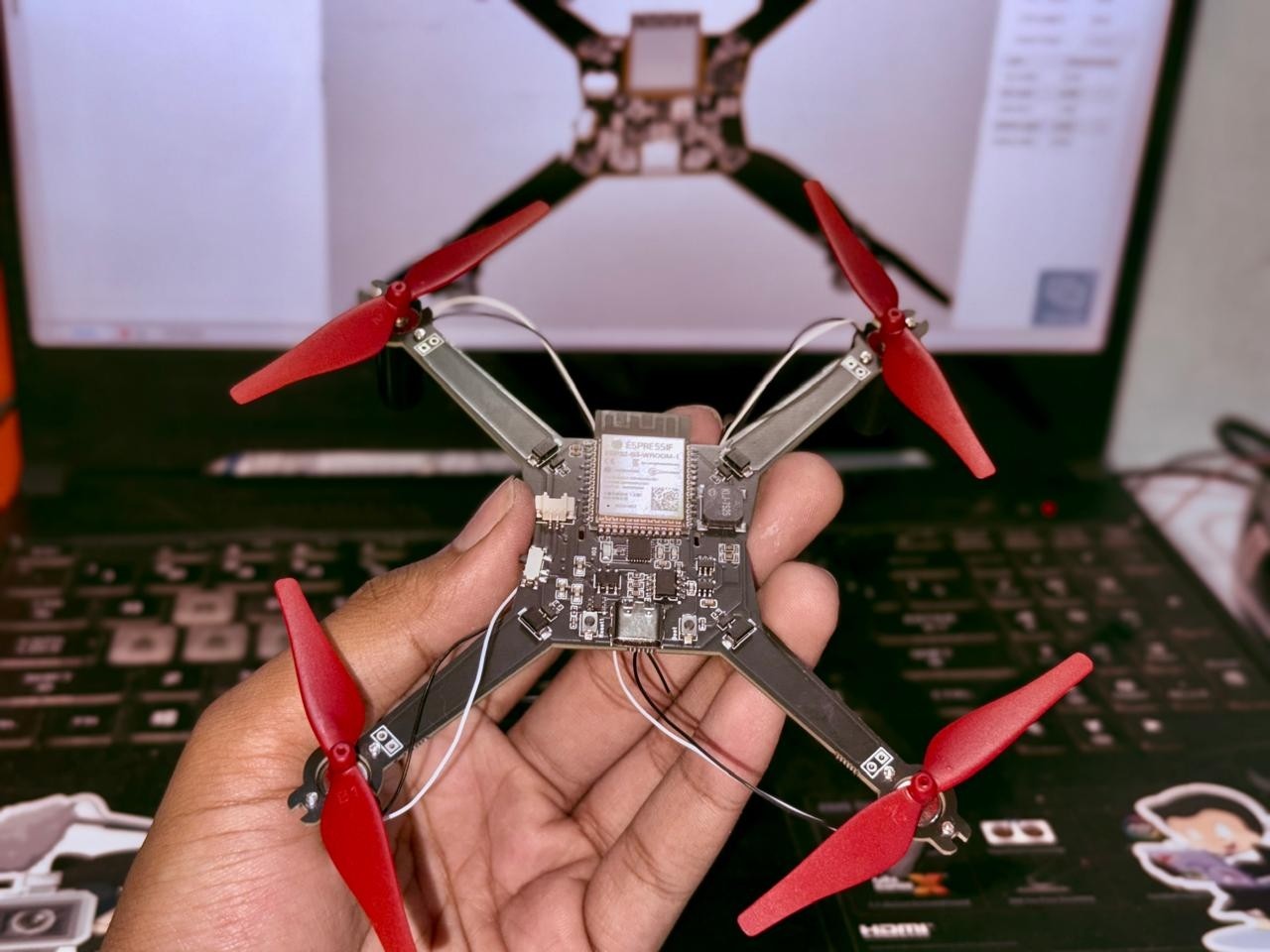
Results & Outcome: A Fully Operational Flight Controller
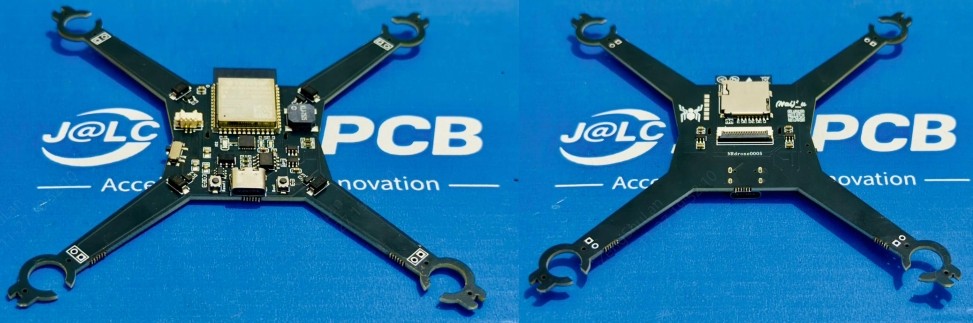
Remarkably, the developer received five fully assembled, double-sided SMT boards ready for testing in just 7 days, despite the order's complexity.
The "moment of truth" arrived with the initial power-up. Each subsystem was then methodically tested by the engineer:
- Manufacturing Precision: The complex "drone-frame" PCB shape was milled perfectly, with all dimensions matching the CAD file. Crucially, the double-sided SMT assembly was perfectly aligned on this non-rectangular board.
- Power System: All three power rails (3.3V, 2.8V, 1.5V) were measured and found to be stable and correct. The complex charging and protection system on the board's underside functioned as designed.
- Core System: The ESP32-S3 booted successfully, and the MPU-6050 was immediately detected on the I2C bus.
- The Crucial Win: The high-speed interfaces, the project's biggest risk, worked on the first revision. The SD-MMC interface (TF Card slot) initialized and operated at its maximum rated speed, allowing for high-speed data logging. The OV2640 camera (via FPC connector) streamed clear video without artifacts or data corruption.
By leveraging JLCPCB's PCBA service, the developer bypassed the entire hardware debugging phase associated with manual SMT assembly, moving directly from unboxing to writing high-level firmware.
Customer Feedback
The engineer's feedback highlights the value of an integrated PCBA ecosystem for complex projects.
"The fast turnaround time was a game-changer. For a complex, double-sided PCBA order, I had the finished boards in my hands in about a week. This speed is critical for rapid prototyping."
"The PCBA quality was perfect. With 2-sided SMT, especially with fine-pitch SMD parts like QFNs and 0402 passives on both sides, the potential for error is high. This was even more of a risk on the complex 'drone-frame' shape. The boards I received had zero solder bridges or assembly defects, and the milling was precise. The fact that all high-speed lines worked on the first revision is a testament to this precision"
"The in-stock parts of JLCPCB made this possible. Having all the unique SMD components, as well as all the power ICs and connectors, supplied from one supplier saved me weeks of logistical work and de-risked the entire build."
FAQ about Mini Drone PCB
Q: Why was the ENIG finish required for the SMT assembly on this Mini Drone PCB Project?
Although standard HASL is more economical, it can create an uneven surface. A design that utilizes fine-pitch QFN and 0402 SMD components needs a perfectly flat, planar surface. The ENIG provides for the solder paste stencil to sit flat, to minimize the chance of solder bridges, and to guarantee that every pad on the fine-pitch SMD parts forms a reliable connection during reflow.
Q: What does "DFM-first" workflow mean in practice for this Mini Drone PCB Project?
It means the engineer's first step was browsing the JLCPCB Parts Library, not the schematic. The entire electronic design (schematic and layout) was bound from the outset to only use SMT components that were confirmed as "In-Stock" and verified for assembly. This is the opposite of the traditional workflow, where sourcing occurs after the PCB design is completed.
Q: What makes double-sided SMT assembly a challenge?
Double-sided PCBA requires two full assembly cycles—one for the top side and one for the bottom side. This means applying solder paste twice, performing two Pick-and-Place (PNP) operations, and running two separate reflow processes.
The challenge lies in managing the second reflow: components that were already soldered on the first side are exposed to heat again when the board goes through the oven a second time. Engineers must carefully control reflow profiles, component orientation, and placement to ensure that parts on the first side do not shift, re-melt, or sustain thermal damage.
Q: Can JLCPCB's PCBA service handle complex-shaped (non-rectangular) boards?
Yes. As this case study demonstrates, the fabrication service can precisely mill complex contours (like the drone frame). The SMT assembly lines are equipped to handle and perfectly align these non-rectangular boards for both single and double-sided PCBA.
Conclusion: High-Density SMT for Mini Drone PCB
This case study shows how JLCPCB's services bridge the gap between ambitious designs and functional prototypes in the real world. By using the PCBA service (for SMT precision and quality, even with double-sided designs) and a massive library of in-stock SMD parts (for logistics and sourcing), engineers can take on real, dense high-speed designs with confidence in their targeted PCB assembly outcomes.
This project demonstrates that even with cost-effective 2-layer PCBs, achieving reliable SMT assembly and sourcing SMD components is absolutely feasible. By leveraging an integrated workflow, developers no longer need to worry about hardware PCBA challenges or the logistics of sourcing SMT components. Instead, they can stay focused on the firmware and system code that bring their innovative designs to life.
Keep Learning