Build Your First Custom PCBA Successfully in 5 Key Steps
13 min
- Step 1: Finalizing Your Custom PCBA Design and Generating Manufacturing Files
- Step 2: Plan Your Component Sourcing for Custom PCB Assembly
- Step 3: Conduct DFM Review and Get an Accurate Custom PCBA Quotation
- Step 4: Follow the Automated PCBA Manufacturing Process
- Step 5: Perform Quality Testing and Final Custom PCBA Delivery
- Conclusion
- FAQs
Moving a design from a bare printed circuit board (PCB) to a fully populated PCBA is an important milestone in any electronics project. It is the point at which a theoretical design becomes an operating piece of hardware.
In this article, you will learn the five most important steps to create and order your first custom PCBA. The entire process will be broken down - we will ensure you make it all the way to a successful outcome. By utilizing an integrated PCB assembly manufacturer like JLCPCB, you can streamline logistics and reduce time to market, from PCB fabrication to final PCB assembly.
To provide a clear roadmap, here are the five key stages we will cover in detail:
1. Design Finalization and File Generation: Preparing your essential Gerber, BOM, and CPL (Component Placement List) files.
2. Component Sourcing Strategy: Choosing between a comprehensive turnkey PCB assembly and consigned PCB assembly service.
3. DFM Review and Quoting: Verifying your design for manufacturability and receiving an instant quote.
4. The Automated Manufacturing Process: A look into how your board is professionally assembled.
5. Quality Control, Testing, and Delivery: The final checks that guarantee a functional product.
Step 1: Finalizing Your Custom PCBA Design and Generating Manufacturing Files
The quality and accuracy of your final custom PCBA are fundamentally determined by the quality of your manufacturing files.
This initial step is the most critical in the whole process, as mistakes created here will naturally create expensive and time-consuming problems along the way. That's why accuracy is vital.
The three key files you receive from your Electronic Design Automation (EDA) software are the Gerbers, Bill of Materials (BOM), and Component Placement List (CPL) file.
#1 Gerber Files: The Blueprint of Your PCB
Gerber files are the industry standard for PCB production. Gerber files are a set of 2D vector image files, where each file is considered a layer of your PCB. When the manufacturer receives your Gerber files, they are not interpreting your original design file; they see the exact patterns to etch, coat, and drill.
To place a successful custom PCBA order, the following layers are required without exception:
● Copper Layers (Top/Bottom): GTL (Gerber Top Layer) and GBL (Gerber Bottom Layer), define the circuit traces, pads, and the copper pours.
● Solder Mask Layers (Top/Bottom): GTS (Gerber Top Solder Mask) and GBS (Gerber Bottom Solder Mask), define where to NOT apply the green (or other color) protective solder mask coating, in order to expose copper pads for soldering.
● Silkscreen Layers (Top/Bottom): GTO (Gerber Top Overlay) and GBO (Gerber Bottom Overlay), contain the text and component outlines (e.g., reference designators, R1, C1, U1).
● Solder Paste Layers (Top/Bottom): GTP (Gerber Top Paste) and GBP (Gerber Bottom Paste) are particularly important for Surface Mount Technology (SMT) assembly and define exactly where solder paste will be applied on the board by stencil before the components are placed.
In addition to these layers, you will need to make a drill file, usually in the Excellon format (e.g., Project.TXT or Project.DRL), that clearly defines where and the size of each hole to be drilled in the board.
#2 Bill of Materials (BOM): Your Component List
The BOM is the master document that tells the assembler exactly which components to place on the board. A poorly formatted or ambiguous BOM is a primary cause of PCB assembly delays. Your BOM, typically a .csv or .xls file, must contain at a minimum:
● Reference Designator: The unique identifier for each component on the silkscreen (R1, C1, U1, etc.).
● Manufacturer Part Number (MPN): The exact, complete number provided by the component manufacturer. Using an internal, or generic, part number will result in sourcing errors.
● Quantity: The total count for each specific component.
● Description/Value: A short description such as the value of the component (e.g, 10k Ohm, 0.1uF).
The best way to optimize PCBA efficiency and cost is to design-in readily available components. Before finalizing your design, it is strongly recommended to review the components you have chosen in the extensive in-stock Parts Library from JLCPCB, which has over 350,000 in-stock components, to assemble your custom PCB, considerably reducing cost and lead times by removing the delays that can occur in sourcing components.
| Reference Designator | Manufacturer Part Number | Quantity | Description |
|---|---|---|---|
| C1, C2, C5 | C0603C104K5RACTU | 1 | 0.1uF 50V X7R |
| R1, R2 | RC0603FR-0710KL | 3 | 10k Ohm 1% |
| U1 | ATMEGA328P-AU | 4 | 8-bit AVR MCU |
Sample Bill of Materials table for a custom PCBA
#3 CPL File (Pick and Place File): Component Coordinates
The Component Placement List (CPL) file, also known as a Pick-and-Place or XY file, is the map for the automated SMT assembly machines. This simple text file (.csv or .txt) contains the precise Cartesian coordinates and rotational orientation for every surface-mount component.
The machine's robotic arm uses this data to pick up each component from its reel and place it on the corresponding pads on the PCB with incredible speed and accuracy. Essential columns include Reference Designator, Layer (Top/Bottom), X-location, Y-location, and Rotation (in degrees).
Step 2: Plan Your Component Sourcing for Custom PCB Assembly
After you have completed your design files, the next thing to think about for your custom PCBA is how you will buy the physical components. This decision directly affects the speed, the cost, and the complexity of your custom PCBA order.
Turnkey PCB Assembly vs. Consigned/Kitted PCB Assembly
● Turnkey PCB Assembly: This is the most efficient and common option for developing electronics in today's world. In the turnkey model, the assembly house - JLCPCB in this instance - assumes all responsibility for purchasing the parts identified in your bill of materials (BOM). They will utilize their own vendor relationships and volume purchasing power to acquire genuine parts at a lower cost than an individual engineer could.
From the customer's perspective, the process is very simple: you give them the files and receive a finished product. For almost all custom circuit board assembly projects, this path is strongly encouraged, as it alleviates the logistical headache of sourcing, planning, and shipping dozens (or hundreds) of random components.
● Consigned/Kitted PCB Assembly: Under a consigned model, you, the customer, will be responsible for sourcing and delivering all or part of the components to the assembly house.
Consigned PCB assembly is less common today, though it is sometimes necessary because some designs may incorporate components that are either proprietary, highly specialized, or otherwise pre-programmed and simply are not available in the open market.
This method does have its advantages in terms of control, but places greater logistics responsibilities on you, the potential for delays due to back-orders of parts, and the responsibility to ensure that all parts are properly and successfully packaged for the automated assembly machines to use.
Tip: For speed, cost-effectiveness, and simplicity, a full Turnkey PCBA service is the superior choice for the vast majority of projects.
Turnkey vs. Consigned custom PCBA processes
Step 3: Conduct DFM Review and Get an Accurate Custom PCBA Quotation
A final check before manufacturing will help validate that your design can be manufactured without any problems. This is when a Design for Manufacturability (DFM) check is important.
The Importance of a Design for Manufacturability (DFM) Check
A DFM check is an automated review of your manufacturing files that can identify potential issues that may interfere with the design, fabrication, and assembly. This is not a check of the function of your circuit, but rather its physical manufacturability. Some common problems identified in a DFM review are:
● Trace to trace or trace to pad clearances that are smaller than allowed.
● Drill hole locations that are too close to copper features or the board edge.
● Solder mask slivers between fine pitch pads.
● Silkscreen text blocking solder pads.
Catching these problems ahead of time can save an enormous amount of time and money. As part of its order process, JLCPCB has incorporated this step into its ordering process with an automated online DFM analysis and will provide the user with feedback as soon as the files are uploaded, allowing the user to address any potential show stoppers before placing the custom PCBA order.
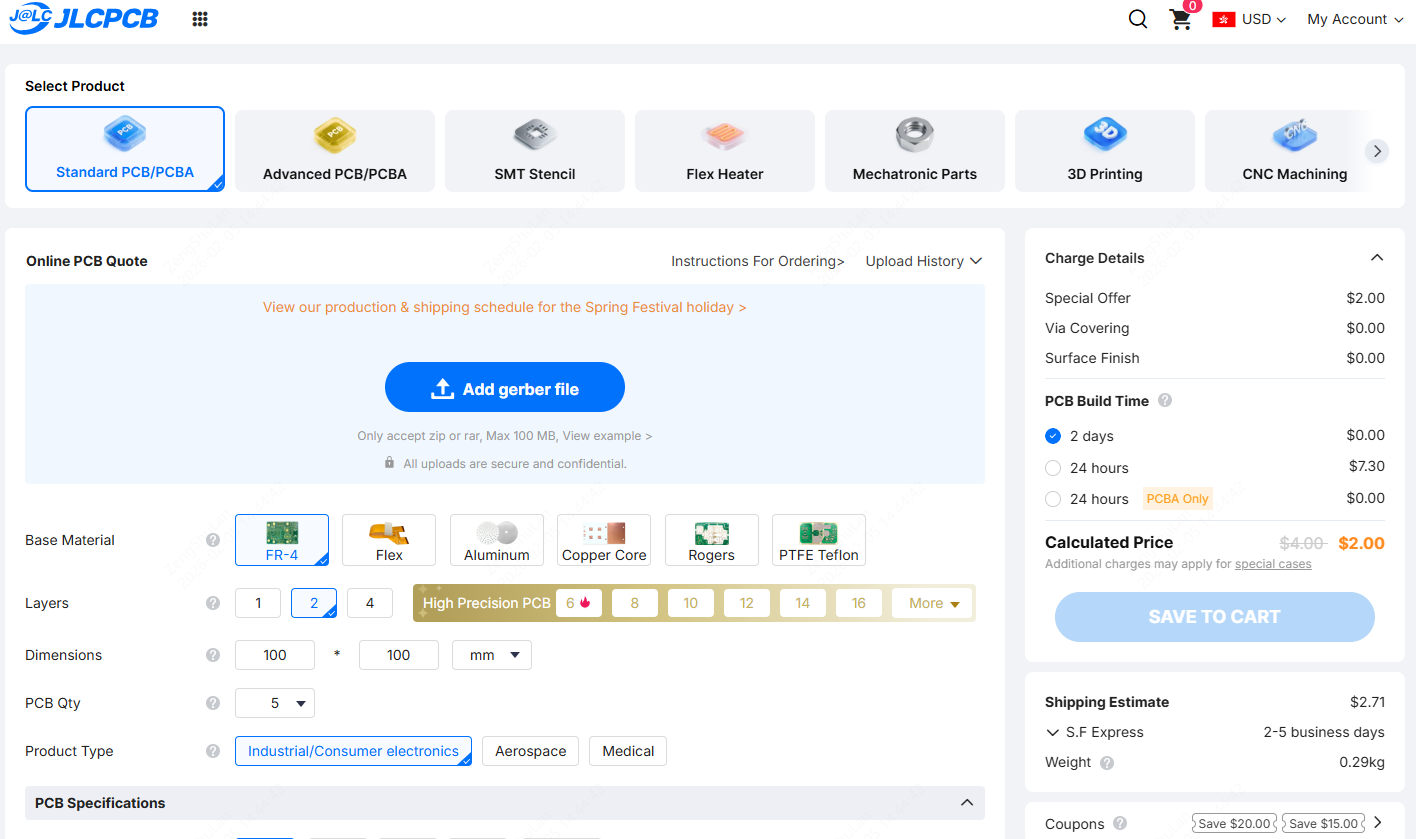
Getting an Instant Online Quote

Once your files are finalized, obtaining a quote for your custom PCBA is easy. Simply upload your Gerber files (in a single .zip file), your BOM, and your CPL file into the online portal. JLCPCB system will extract the data and let you configure your order with options like:
● PCB Quantity
● PCB specifications (layers, material, thickness, color)
● Assembly on the top side, bottom side, or both
The portal provides a fully itemized and transparent quotation, clearly breaking down labor, component, and PCB costs — making it as simple to order a custom PCBA project as ordering a single PCB.
Step 4: Follow the Automated PCBA Manufacturing Process
Once the quote for your custom PCBA has been approved, your design will be taken to a high-volume automated manufacturing facility. Understanding this process will help illuminate the technology that produces your board.
SMT (Surface-Mount Technology) Assembly
SMT Assembly is the core of modern PCBA.
1. Solder Paste Application: A laser-cut stainless-steel stencil, custom-made from your solder paste Gerber files, is carefully aligned and placed over the PCB. A squeegee blade then spreads solder paste evenly and precisely onto the component pads.
2. Pick and Place: The board is then transferred to a high-speed pick and place machine, which uses the CPL file to control a robotic head to pick up individual SMDs from their reels and place them onto their pads on the board at speeds of thousands of components per hour.
3. Reflow Soldering: The populated board travels through a long reflow oven with multiple, precisely controlled temperature zones. The board is gradually heated to activate the flux in the solder paste and then brought to a temperature that melts the solder. As the board cools, the solder solidifies, creating strong and reliable electrical and mechanical connections for all components.
THT (Through-Hole Technology) Assembly
While most components are SMT, some parts like large capacitors, connectors, and power components still use Through-Hole Technology for its mechanical robustness.
1. Component Insertion: Through-hole components are either inserted manually by skilled technicians or by specialized automated insertion machines.
2. Wave Soldering: For boards with many THT components, they may pass through a wave soldering machine. The board travels over a wave of molten solder, which solders all the through-hole leads in a single pass.
The custom PCBA manufacturing process, showing solder paste, pick-and-place, and reflow oven stages.
Step 5: Perform Quality Testing and Final Custom PCBA Delivery
The final step before your custom PCBA is shipped is a rigorous quality control process to ensure every board meets strict standards.
Inspection and Quality Assurance
● Automated Optical Inspection (AOI): Each board is scanned by an AOI machine after reflow soldering. The AOI machine utilizes high-resolution cameras to compare the assembled board with your design data, verifying component placement, polarity, and solder joint quality, as well as identifying any solder bridges.
● X-ray Inspection: X-ray inspection cannot be performed for components located with their leads under their package, such as Ball Grid Arrays or Quad-flat No-Leads, as they cannot be optically inspected. For manufacturers of these components, X-ray inspection is used to see if the solder connections are good, as it can see through the package.
● Functional Testing (FCT): For production runs with a larger quantity of boards, customers may provide a testing procedure and a "bed-of-nails" test jig. This allows an automated functional test to be performed, verifying that each board powers up and functions as designed when the boards leave the factory.
Final Packaging and Shipping
After inspection, the boards are thoroughly cleaned and packaged in an anti-static bag and a secure, padded box to prevent any electrostatic discharge (ESD) or physical damage during delivery. JLCPCB offers a variety of international shipping options so that you will soon receive your high-quality, professionally custom PCBAs ready to integrate into your final product.
Conclusion
Building your first custom PCBA is an easy and simple process when you can break it down into five fundamental steps: proper file creation, thoughtful components sourcing, completing DFM checks, understanding the assembly process, and strong quality control.
With the support of JLCPCB, an integrated PCB fabrication and assembly manufacturer that brings together all five steps in one seamless platform, your concentration can now be simply on what you do well: design electronics. Your project is actually much closer to reality than you think, and within reach of bringing your digital design to a physically populated board.
Ready to bring your design to life? Get an instant quote for your custom PCBA project at JLCPCB today!
FAQs
Q: What is the minimum order quantity (MOQ) for a custom PCBA order?
JLCPCB is geared for prototyping and small to medium-volume production, with an exceptionally low MOQ starting at just 2 pieces for SMT assembly, making it highly accessible for individuals and small businesses.
Q: How do I handle components for my custom PCBA that are not in the JLCPCB parts library?
If your design requires a part not in the in-stock library, you can use the consigned PCB assembly option. You would source these specific components yourself and send them to JLCPCB to be included in the assembly process.
Also Read: How to consign parts to JLCPCB
Q: What is the typical turnaround time for a turnkey custom PCBA order?
Turnaround times can vary based on component sourcing lead times and assembly complexity, but for projects using readily available components from the JLCPCB parts library, production can often be completed in just a few days.
Q: Can JLCPCB handle a custom PCBA with complex components like BGAs?
Yes. The automated SMT assembly lines are equipped to handle high-density and complex components, including Ball Grid Arrays (BGAs) and fine-pitch QFP/QFN packages. X-ray inspection is used to ensure the quality of solder joints for these bottom-terminated components.
Q: What file formats are accepted for the BOM for a custom PCBA order?
For seamless integration with the online quoting system, the Bill of Materials should be provided in a standard spreadsheet format, such as .csv, .xls, or .xlsx.
Popular Articles
• How to Design and Assemble a Reliable ESP32 Module PCB on a 2-Layer Board
• The Ultimate Guide to Relay Symbol: Coil, Contacts, Diagrams, and Circuit Applications
• How to Identify SMD LED Polarity: Markings, Testing, and PCB Tips
• The Ultimate Guide to PCBA: Process,Types and Techniques for the Electronics Enthusiast
• How to Create a Bluetooth-Controlled Car With Arduino: A Step-by-Step Guide
Keep Learning
Diode Voltage Drop: Values, Formula, and How to Measure It
Every diode loses some voltage when it conducts. That loss is the diode voltage drop, and it decides how much voltage reaches your load, how much heat your part makes, and whether your low-voltage rail still works. This guide covers typical forward voltage by type, the formula behind it, what changes it, how to measure it with a multimeter, and why it matters in real circuits. What Is Diode Voltage Drop? Diode voltage drop is the forward voltage (Vf) that appears across a diode when current flows from......
The Ultimate Guide to Testing Diodes: Multimeter Settings, Readings, and Diagnosis
Quick Answer: How to Test a Diode To check a diode with a multimeter, set the device to diode test mode. Put the red probe on the anode and the black probe on the cathode. A healthy silicon diode provides a good diode reading of 0.5V to 0.8V in forward bias and OL (Open Loop) in reverse bias. Knowing how to tell if a diode is bad is simple: OL both ways indicates an open diode, while a near-zero voltage reading both ways indicates a shorted diode. Knowing how to test a diode is one of the fastest ways......
Arduino LED Driver Tutorial: Control More LEDs with 74HC595 and MAX7219
Arduino GPIO pins run out quickly in larger LED projects. By utilizing dedicated LED drivers and expansion ICs, you can drastically reduce pin usage, eliminate processor-heavy multiplexing loops, and simplify display wiring. In this guide, you will learn the operational architecture, wiring configurations, cascading techniques, and optimization strategies for the 74HC595 shift register and the MAX7219 LED driver. Why Arduino Projects Need LED Driver ICs Arduino GPIO and Current Limitations An ATmega32......
How to Design and Assemble a Reliable ESP32 Module PCB on a 2-Layer Board
Many engineers fail when designing their first ESP32 PCB due to antenna issues, power instability, or SMT defects. Designing a custom board with an ESP32 Module strikes the perfect balance between customizability and ease of manufacturing. Unlike a chip-down design, the module integrates the crystal oscillator, flash memory, and RF matching network, reducing the PCBA risk significantly. the SMD package (for example, ESP32-S2-WROOM modules) introduces several assembly considerations, including pad sold......
How to Read a MOSFET Symbol: NMOS, PMOS, Arrows, and Body Diodes
If you have ever opened a schematic and stared at a MOSFET symbol wondering which terminal is the source, why the gate has a gap, or why the arrow points differently on two seemingly identical symbols — you are not alone. The MOSFET schematic symbol packs four independent pieces of information into one small graphic: channel polarity, operating mode, terminal identity, and device type. Read those four cues correctly, and any MOSFET symbol becomes immediately clear, whether you encounter it in a power-......
Circuit Breaker Symbols Explained: IEC, ANSI, MCB, and Pole Configuration Symbols
Electrical schematics are the universal language of power systems, control circuits, and printed circuit boards. Within these diagrams, the circuit breaker symbol is one of the most critical elements. Getting it right is essential for safety, troubleshooting, and manufacturing. An error as simple as mixing up a circuit breaker with a manual switch or an isolator can lead to catastrophic misinterpretations on the factory floor or during field maintenance. This guide provides a complete, technically acc......