Blind Via
Connects an outer copper layer to an internal copper layer without passing through the full board thickness. JLCPCB forms HDI blind vias by laser drilling.
Build high-density interconnect PCBs that pack more routing into less board space.
PCB Coupon · 6+ Layers
Claim $35 CouponPCB Coupon · 4 Layers
Claim $10 CouponJLCPCB HDI PCB fabrication capability supports 4–24 layer boards, up to 3rd-order HDI structures, laser-drilled blind vias, mechanically drilled buried vias, fine-line routing, and controlled-impedance requirements. Review these HDI PCB design guidelines before requesting a quote.
Capability/design rule | Production capability | Conditions and engineering notes |
|---|---|---|
HDI base materials | Shengyi S1000-2M or Nan Ya NP-175F; Tg 170°C | FR-4 only. Capability material notes: Anti-CAF, good dimensional stability, low shrinkage. |
Supported HDI structures | 1st-, 2nd-, and 3rd-order HDI | Supports structures with or without mechanically drilled buried vias. Cross-layer laser-via structures, such as L1–L3 or L6–L4, are supported as skip-via designs; they are manufactured as stacked blind/buried-via structures. |
Layer count | 4–24 layers | Applicable to blind/buried-via HDI boards. |
Finished board thickness | 0.5–3.0 mm | 0.5 mm is limited to 4-layer boards. Tolerance: ±0.10 mm for finished boards below 1.0 mm; ±10% for finished boards at or above 1.0 mm. |
Laser drilling process | Laser direct drilling | Used for laser-drilled blind vias. |
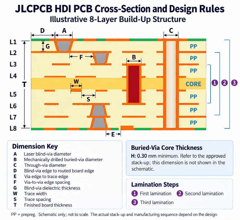
Laser blind-via diameter | 0.075–0.150 mm | Default laser-via diameter is 0.10 mm unless otherwise specified. A 0.175 mm laser-via option is unavailable so far. |
Mechanically drilled buried-via diameter | 0.15–0.55 mm | Buried vias use resin plugging and copper capping. Extreme capability: 0.10 mm when the mechanically drilled dielectric span is ≤1.0 mm. Mechanical via aspect-ratio rules apply. |
Orderable board and panel size | Board: 5 × 5 mm to 576 × 469 mm | Minimum V-cut panel size: 30 × 60 mm. Smaller panels require tab-routing/stamp-hole panelization. |
Controlled-impedance tolerance | ≥50 Ω: ±10%; <50 Ω: ±5 Ω | For example, 45 Ω is controlled to 45 ±5 Ω. |
Bow and twist | ≤0.75% | IPC Class 2 standard. |
Capability/design rule | Production capability | Conditions and engineering notes |
|---|---|---|
Lamination and pressing | Buried-via core thickness: ≥0.30 mm; pressed PP thickness: ≥50 μm | The 0.30 mm minimum applies to the core across the buried-via span and supports via plugging and plating. |
PP options for laser vias | Available nominal laser-drilled blind-via diameters: 75, 100, 125, and 150 μm | Laser-drillable prepreg (PP) examples: 1078/1080 RC69, 86 μm (3.39 mil); 106 × 2 RC72, 50 μm (1.97 mil) × 2; 2313 RC58, 103 μm (4.06 mil) ; 2116 RC57, 150 μm (5.91 mil). Final PP selection is stack-up dependent and requires DFM confirmation. |
Hole-diameter tolerances | PTH component holes / through holes: ±0.0762 mm (3 mil); NPTH component holes: ±0.0508 mm (2 mil); | / |
Via filling, plating, and aspect ratio | Laser blind-via aspect ratio: ≤1:1; mechanical buried-via and through-hole aspect ratio: ≤16:1 Actual availability is subject to the configurations supported on JLCPCB’s online ordering page. | Laser blind vias are copper filled and planarized. Blind-via filling diameter: 0.075–0.150 mm. Maximum blind-via fill recess: 25.4 μm. |
Trace capability and outer-layer copper | Standard minimum artwork line / space: 3.0 / 3.0 mil | Extreme capability: 2.7 / 2.7 mil, subject to higher process difficulty and cost. |
Laser-via capture pad | Pad diameter = laser-via diameter + 6 mil | Minimum annular ring: 3 mil per side. |
Laser-via aperture | 0.075–0.150 mm | Laser-drilled blind vias. |
Laser-via target pad | Pad diameter = laser-via diameter + 6 mil | Minimum annular ring: 3 mil per side. |
Blind-via-to-via spacing | Same net: ≥5 mil / 0.13 mm; different nets: ≥9.5 mil / 0.24 mm | Applies to spacing between blind vias and relevant blind, buried, or through-via features. |
Inner-layer mechanical buried-via aperture | 0.15-0.55mm | Applies to mechanically drilled buried vias using the resin-plugging process. |
Mechanical buried-via pad | Pad diameter = buried-via diameter + 6 mil | Minimum annular ring: 3 mil per side. |
Laser blind-via to board-edge clearance | ≥14 mil / 0.35 mm | Clearance is measured from the blind-via edge to the routed board edge. |
Outer-layer via-edge to trace-edge clearance | Different nets: ≥6 mil | Values below 6 mil require engineering review. |
Inner-layer via-edge to trace-edge clearance | ≥6 mil | Values below 6 mil require engineering review. |
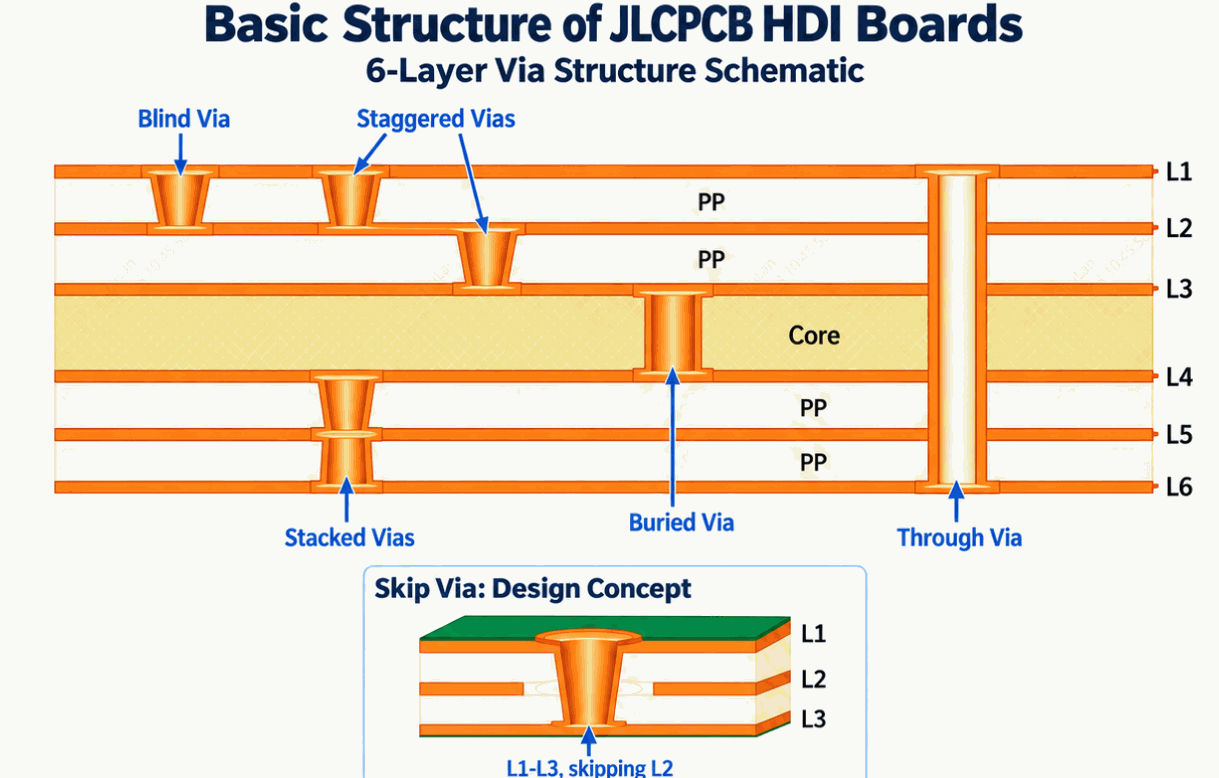
Connects an outer copper layer to an internal copper layer without passing through the full board thickness. JLCPCB forms HDI blind vias by laser drilling.
Connects internal copper layers without extending to either outer surface of the finished PCB.
Extends through the full board thickness, from the top layer to the bottom layer. JLCPCB forms through vias by mechanical drilling.
Vias on successive layer spans that are vertically aligned and electrically connected along the same axis.
Vias on successive layer spans that are laterally offset and connected by copper routing on an intermediate layer.
A blind via that spans two or more dielectric layers, bypassing at least one intermediate copper layer—for example, an L1–L3 via that skips L2.
JLCPCB’s in-house factories use optical inspection of laser-drilled vias and four-wire (Kelvin) low-resistance testing to check via quality and identify abnormal interconnect resistance.
Laser-drilled blind vias and fine-line routing help you connect selected layers without using through vias for every transition, creating more options for routing around fine-pitch components.
JLCPCB copper fills and planarizes laser blind vias to support reliable interlayer connections and provide flat, solderable pad surfaces for via-in-pad assembly. Mechanically drilled buried vias are resin plugged and copper-capped to support dense multilayer interconnections.
Tg 170°C laminates from Shengyi and Nan Ya provide specified material options for HDI construction. Known material grades give engineers a clear basis for material selection and stack-up planning.
JLCPCB reviews HDI orders before payment, so you can confirm your stack-up, any required impedance-control plan, and final pricing with our engineering team before paying.
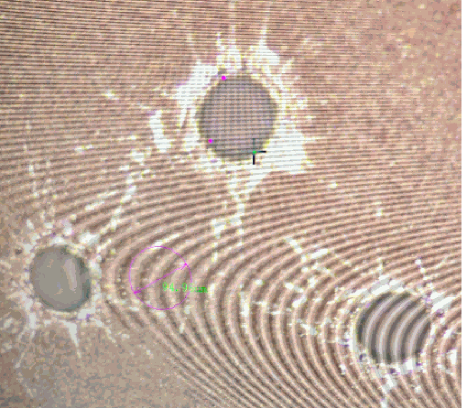
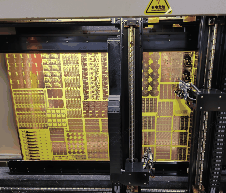
Fine traces, compact pads, and microvias help fit more connections into limited board space. These features also provide more options for fine-pitch BGA escape routing.
Blind and buried vias connect selected layers without extending through the full board thickness, giving designers more flexibility when planning multilayer routing.
Choose fabrication only or add PCB assembly. Both workflows include engineering review before payment.
Upload your Gerber ZIP file on the online quote page. The system automatically detects your board dimensions and layer count.
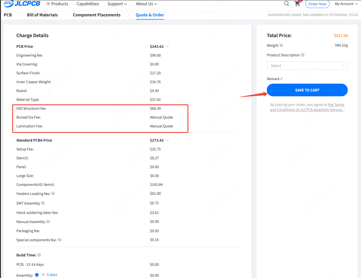
Select HDI under Base Material, then confirm your layer count, board thickness, surface finish, and other specifications. The Charge Details section automatically updates the cost breakdown as you adjust your selections. Blind/buried-via and lamination charges are confirmed after engineering review.
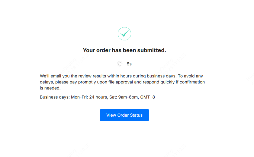
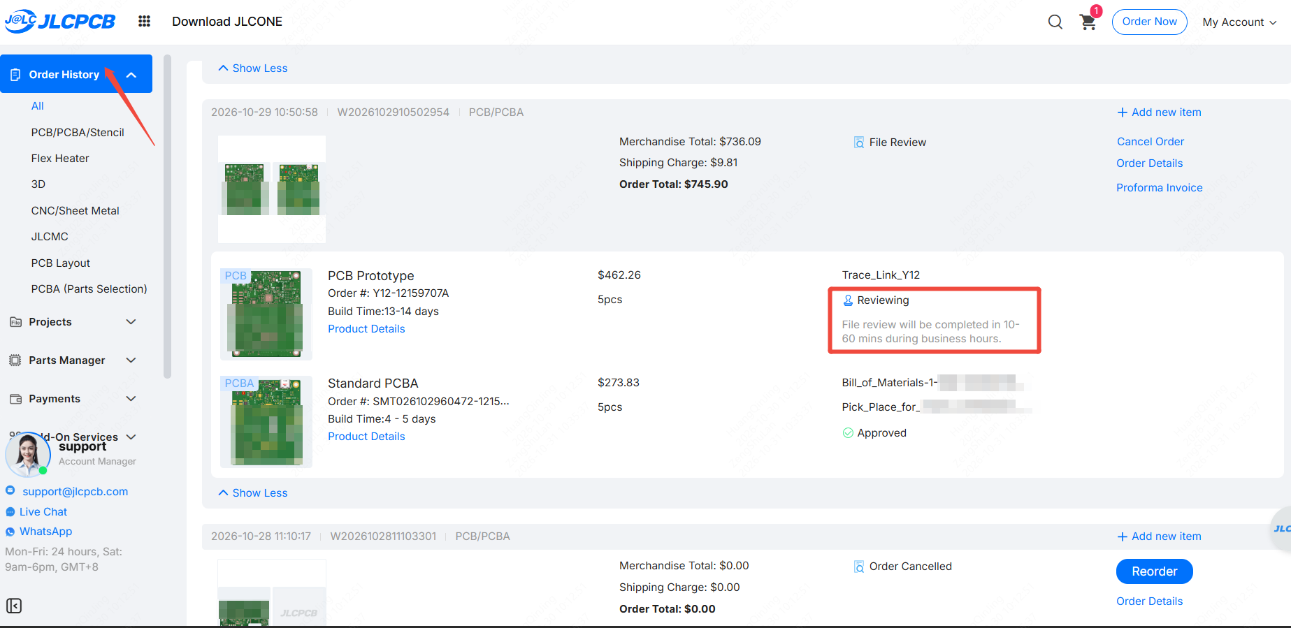
Add your PCB order to the cart and submit it for engineering review. Reviews are typically completed within a few hours on business days, and you’ll receive the result by email or check the status in the Order History section.
Once approved, complete payment to release your order for production. You can track production progress and shipping status on the order page.
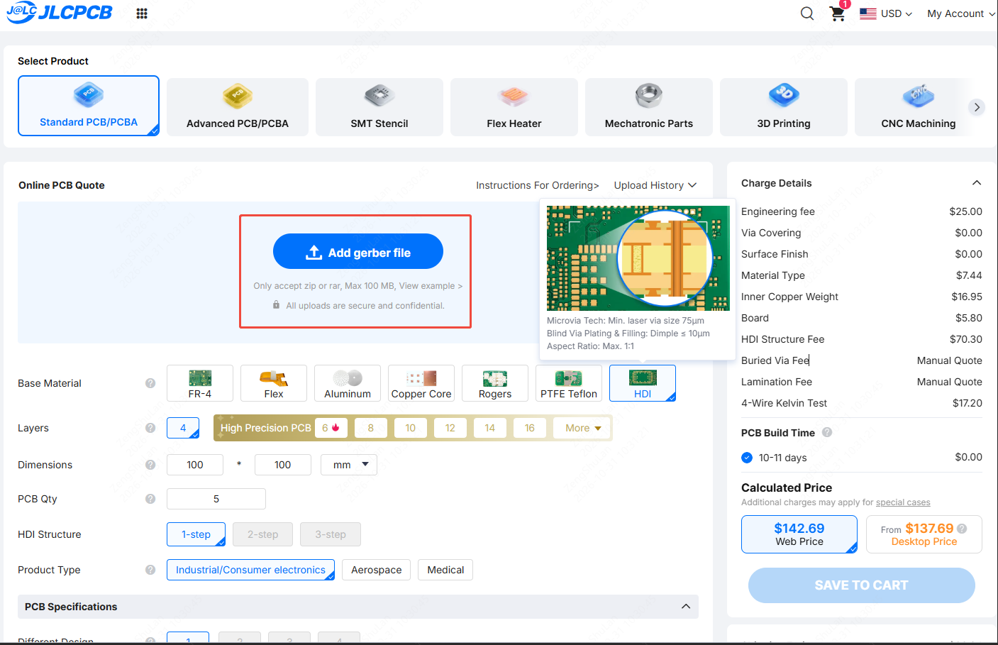
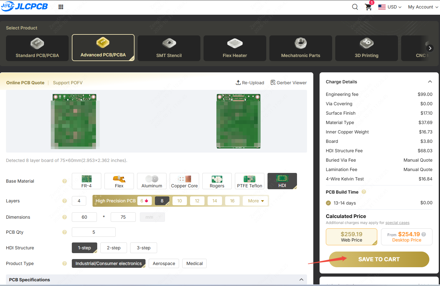
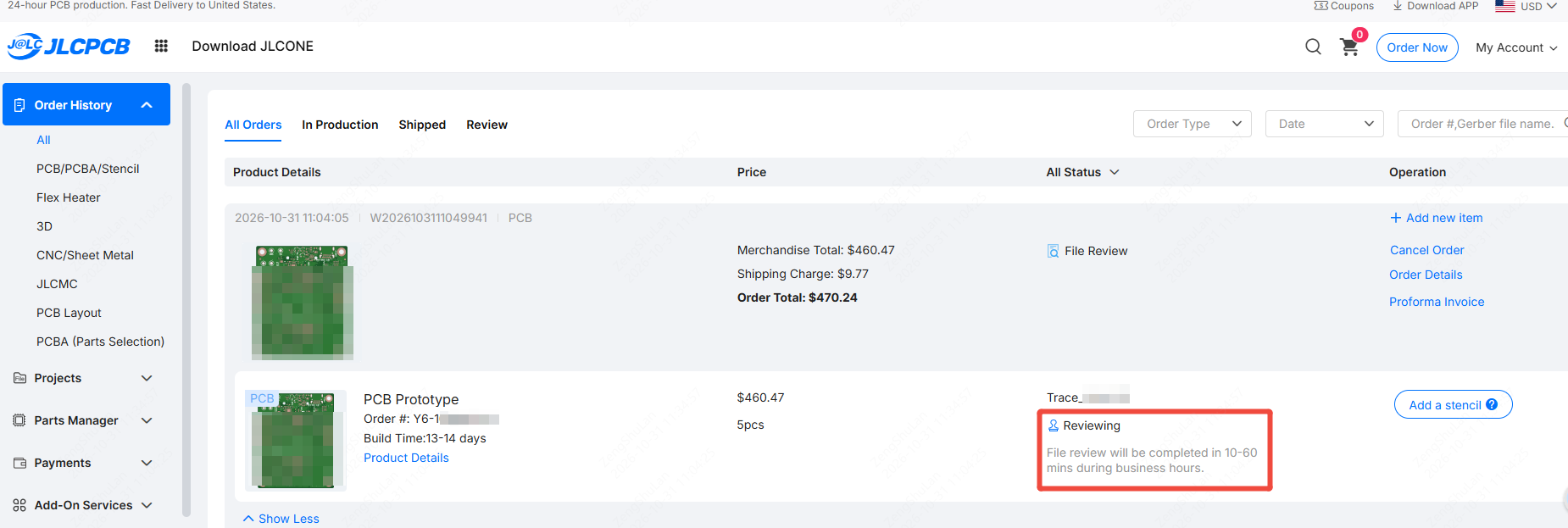
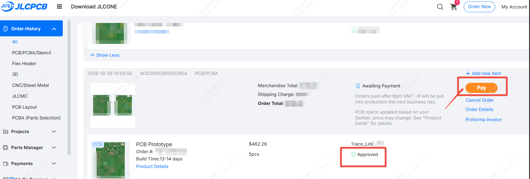
Upload your Gerber files on the online quote page, select HDI as the board material, and confirm your PCB specifications.
Enable PCB Assembly. The system automatically selects Standard PCBA. Click Next to upload your bill of materials (BOM) and component placement list (CPL). The system automatically matches components.
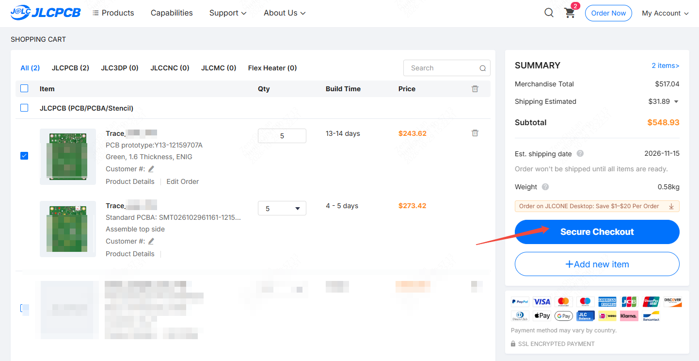
Review the PCB fabrication and assembly cost breakdown in the Quote & Order section. Click SAVE TO CART and then click Secure Checkout to complete the order submission steps.
Our engineers review your PCB and assembly files and notify you by email. You can also check your order status in the Order History section. Once your order is approved, complete payment. We then fabricate and assemble your boards and ship the completed assemblies together.
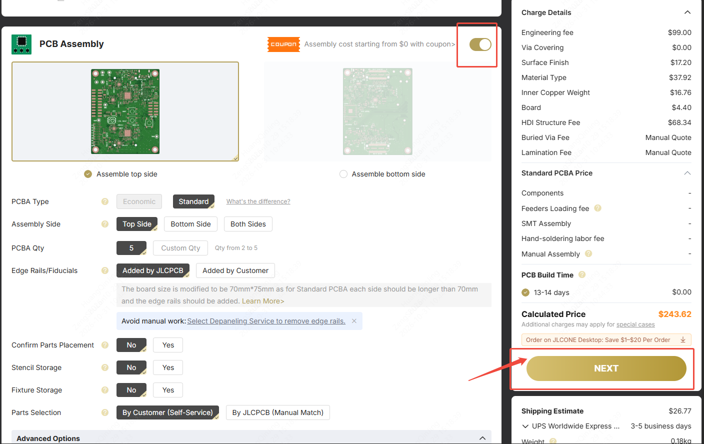
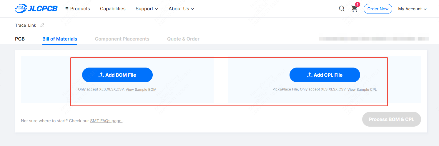
Learn how blind and buried vias increase routing density, support fine-pitch BGAs, and enable more compact electronics.
Watch on YouTubeUpload your Gerber files and select your HDI specifications to get an online quote from JLCPCB.
Get an HDI PCB QuoteExclusive $35 PCB Coupon · Eligible for PCB orders with 6 or more layers.
