HDI High-Density Interconnect PCBs Officially Launched
Last updated on Sep 07, 2026
High-Density Interconnect (HDI) PCBs are a core building block of modern electronic products. With high routing density, miniaturized design, and excellent electrical performance, they are driving rapid innovation in consumer electronics, communication equipment, automotive electronics, and other fields. As 5G, artificial intelligence, and IoT technologies become more widespread, advances in signal integrity, thermal efficiency, and multilayer stack-up technology have made HDI boards a key solution for high-frequency, high-speed transmission. Driven by the wave of digitalization and intelligence, and in response to customers' urgent demand for efficient, stable, and customized solutions, we are officially launching HDI High-Density Interconnect PCBs. This launch is not only a milestone in technology advancement, but also a practical result of our customer-centered philosophy.
HDI Board Features and Applications
Advantages:
1. Optimized routing. Smaller line width/spacing, pads, and microvias improve design efficiency.
2. Better materials and advanced production processes provide improved reliability and stability.
3. Smaller dimensions and footprint, making HDI boards well suited to advanced packaging technologies.
4. Multilayer interconnection supports high standards for electrical performance and efficiency.
Limitations:
The process is complex, repair is difficult, the price is higher, and the lead time is longer.
Application Fields:
1. Smartphones, tablets, digital cameras, MP3 players, MP4 players, and more.
2. Automotive electronics, aerospace, and medical equipment.
3. Communication equipment and network equipment.
Basic Structure of JLCPCB HDI Boards
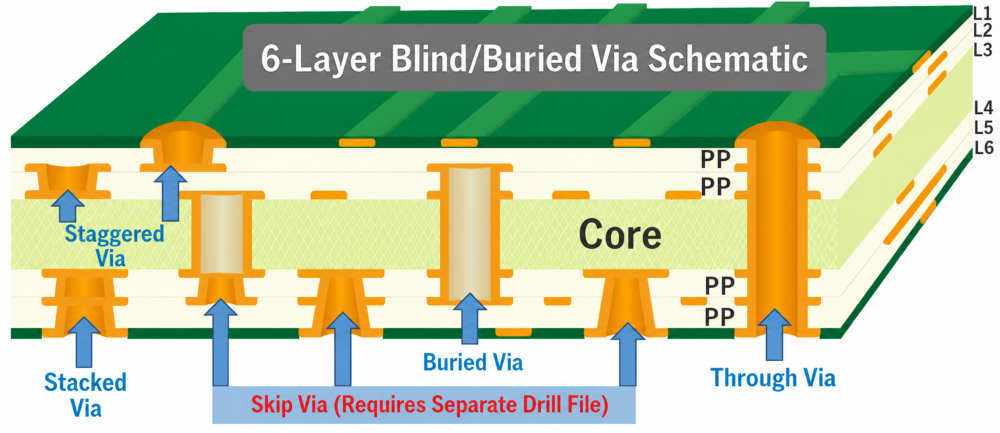
Blind via: A via that connects the top or bottom layer to an inner layer without passing through the entire board. It is formed by laser drilling and supports 1st-order, 2nd-order, and 3rd-order HDI.
Buried via: A via that connects only traces between inner layers. Neither end of the hole extends to an outer layer, so the via is fully buried inside the board.
Through via: A via that passes through the full board thickness, from the top layer to the bottom layer, and is made by mechanical drilling.
Stacked via: Blind and buried vias aligned at the same vertical position, with copper plating between vias. Different laminated structures are manufactured according to the via type.
Skip via: A blind via that skips across two or more layers. During production, it is split into stacked blind and buried vias.
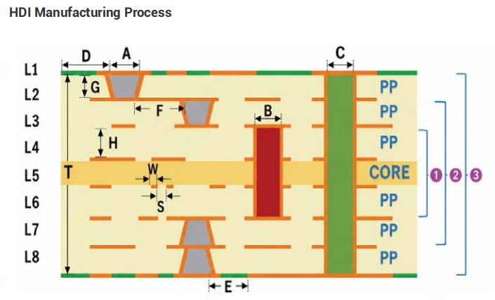
JLCPCB HDI Board Manufacturing Process
HDI Board FAQ
1. Q: What laser-drilled hole sizes can JLCPCB make for HDI boards? Are blind and buried vias plugged or filled?
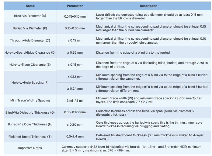
A: The default laser-drilled hole diameter is 0.1 mm. Laser-drilled holes from 0.075 mm to 0.15 mm can be processed.
A: Blind and buried vias are filled. Blind vias are filled and planarized by electroplating, while buried vias are resin plugged and capped with plating.
2. Q: What is the hole diameter tolerance for JLCPCB HDI boards?
A: PTH component hole tolerance is controlled at +/-0.076 mm. NPTH component hole tolerance is controlled at +/-0.05 mm. Via hole diameters are not controlled. Details are as follows:
A: Laser blind vias are filled and planarized by electroplating. Mechanical buried vias use resin plugging.
3. Q: What is the minimum panel size for JLCPCB HDI boards?
A: With V-cut processing, the minimum panel size is 30 x 60 mm. Panels smaller than this can use stamp-hole panelization.
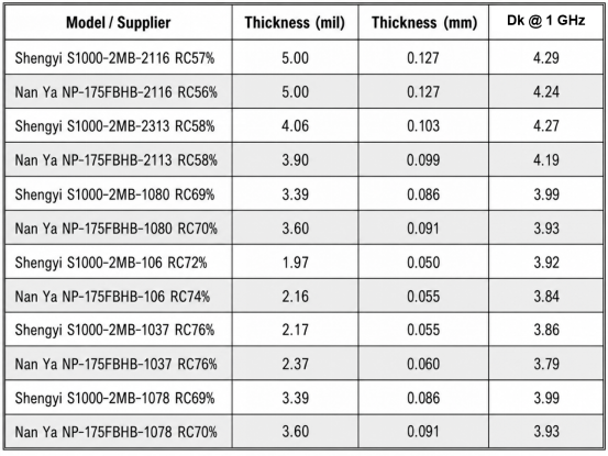
4. Q: What materials are available for JLCPCB HDI boards, and what are the common PP specifications and thicknesses?
A: We use Shengyi and Nanya laminates. The relevant PP parameters are as follows:
5. Q: If the PP layer between L1 and L2 is required to be 0.1 mm thick, can a 0.075 mm blind via be designed?
A: No. The blind-via thickness-to-diameter ratio must be <= 1:1. In other words, with a 0.1 mm dielectric thickness, the minimum blind-via diameter is 0.1 mm.
6. Q: What is the maximum thickness for an HDI board, and what is the corresponding minimum through-hole size?
A: The aspect ratio for mechanical buried vias and through vias must be <= 16:1. We can process HDI boards up to 2.4 mm thick, with a corresponding minimum through-hole size of 0.15 mm.
7. Q: What is the tolerance for impedance control? What is the impedance tolerance for 45 ohms?
A: When the impedance value is >= 50 ohms, the tolerance is +/-10%. When the impedance value is < 50 ohms, the tolerance is +/-5 ohms. For example, the tolerance for 45-ohm impedance is 45 +/-5 ohms.
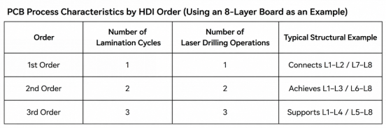
8. Q: How are 1st-order, 2nd-order, and similar HDI boards distinguished?
A: The distinction between 1st-order to 3rd-order PCB structures is mainly based on the number of lamination cycles and laser drilling operations. 1st-order means one lamination cycle and one laser drilling operation; 2nd-order means two
lamination cycles and two laser drilling operations; 3rd-order means three lamination cycles and three laser drilling operations, and so on. The PCB order is determined by two key indicators:
(1) Number of lamination cycles: the number of interlayer bonding processes during PCB manufacturing;
(2) Number of laser drilling operations: the number of processing operations used to form blind and buried vias by laser technology;
9. Q: Compared with standard PCBs, what should be considered when designing HDI boards?
A: Please note the following:
1) Blind vias are formed by laser drilling, so the hole diameter cannot be too large. The diameter should be within 0.075-0.15 mm and must also match the corresponding PP layer thickness.
2) The annular ring for blind and buried vias should be at least 0.075 mm, meaning the pad diameter should be at least 0.15 mm larger than the hole diameter. The hole-edge spacing between different nets should be >= 0.24 mm.
3) The minimum line width/spacing is 3/3 mil. When there is enough space, please design at 3.5/3.5 mil. In tight spaces, we support an extreme line width/spacing of 2.7/2.7 mil, but this will increase difficulty and cost.
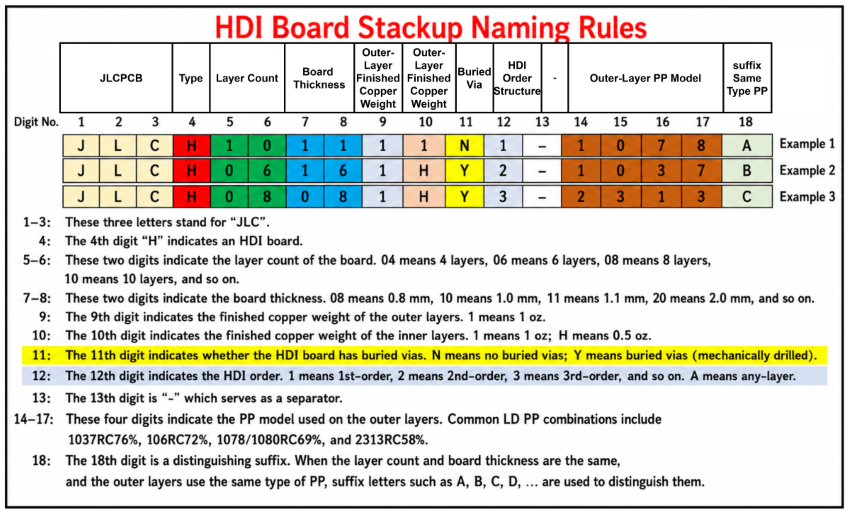
10. Q: When ordering an 8-layer board, the stack-up structure option includes "JLCH081611Y2-1078A". How are these HDI board stack-up structures named?
A: Please refer to the following: