
JLCPCB Showcases Full-Stack Electronic Manufacturing Platform at JPCA Show 2026
Press Release
Jun 10, 2026- About the JPCA Show
- JLCPCB at Booth 3F-29: High-End Capabilities & Integrated Ecosystem
- About JLCPCB
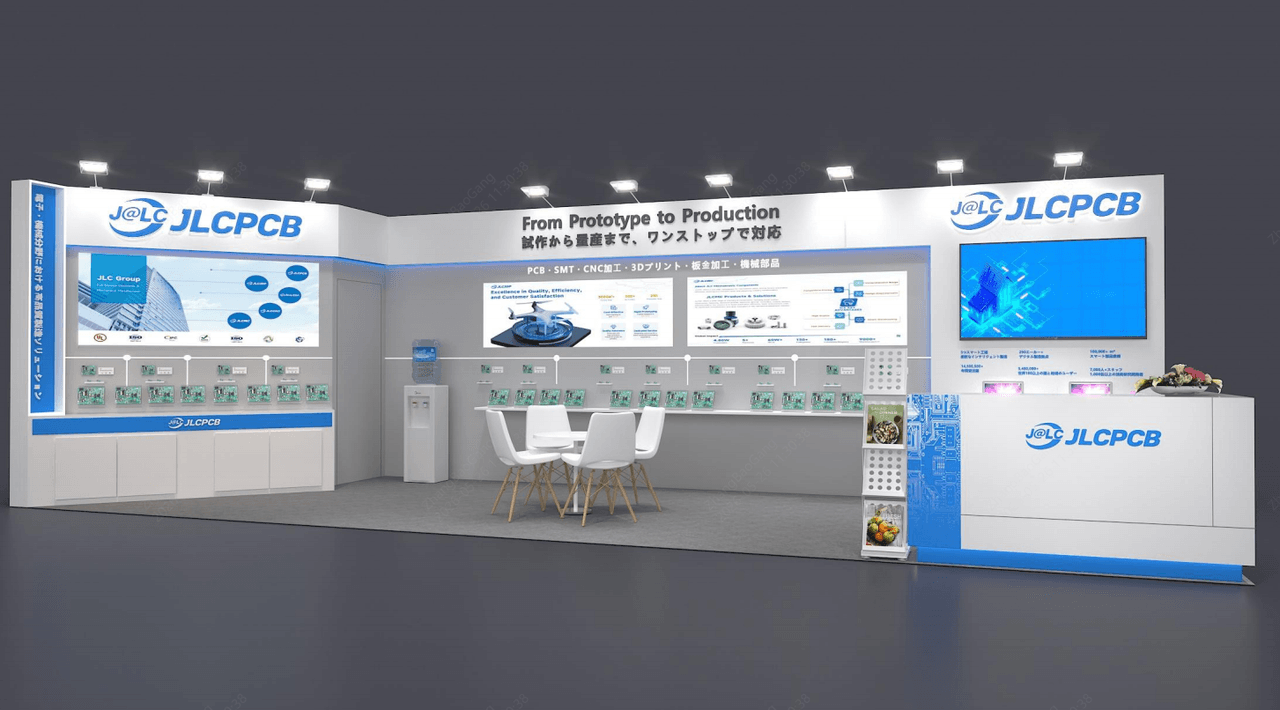
TOKYO, Japan — Today, the JPCA Show 2026 officially opens its doors at Tokyo Big Sight, East Exhibition Halls. JLCPCB, a global leader in electronic manufacturing, welcomes all attendees to Booth 3F-29. We are live on-site showcasing our advanced technologies and integrated hardware ecosystem, enabling engineers, hardware startups, and enterprises to push the boundaries of electronic system design and manufacturing.
About the JPCA Show
JPCA Show 2026 is Asia’s premier electronics event. The exhibition serves as a global hub for advanced circuits, smart manufacturing, packaging technologies, and automotive/industrial electronics, connecting industry leaders and tech innovators worldwide.
JLCPCB at Booth 3F-29: High-End Capabilities & Integrated Ecosystem
Moving beyond simple prototyping, JLCPCB arrives in Tokyo to demonstrate its full spectrum of manufacturing capabilities. Visitors can explore:
- Advanced Manufacturing: 1-32 layer PCBs, supporting high-frequency, high-speed, and flexible PCBs. The minimum drill size is 0.15mm.
- Reliable Quality: In-process AOI, flying probe, 4-wire Kelvin testing, ±10% impedance control.
- Full-Stack Ecosystem: Our full vertical integration spanning EDA → PCB Layout → PCB → Stencil → Component Sourcing → PCBA (SMT Assembly).
- Expert Consultations: Our expert team will be on-site to answer questions, provide insights, and discuss your specific project requirements.
Event Details:
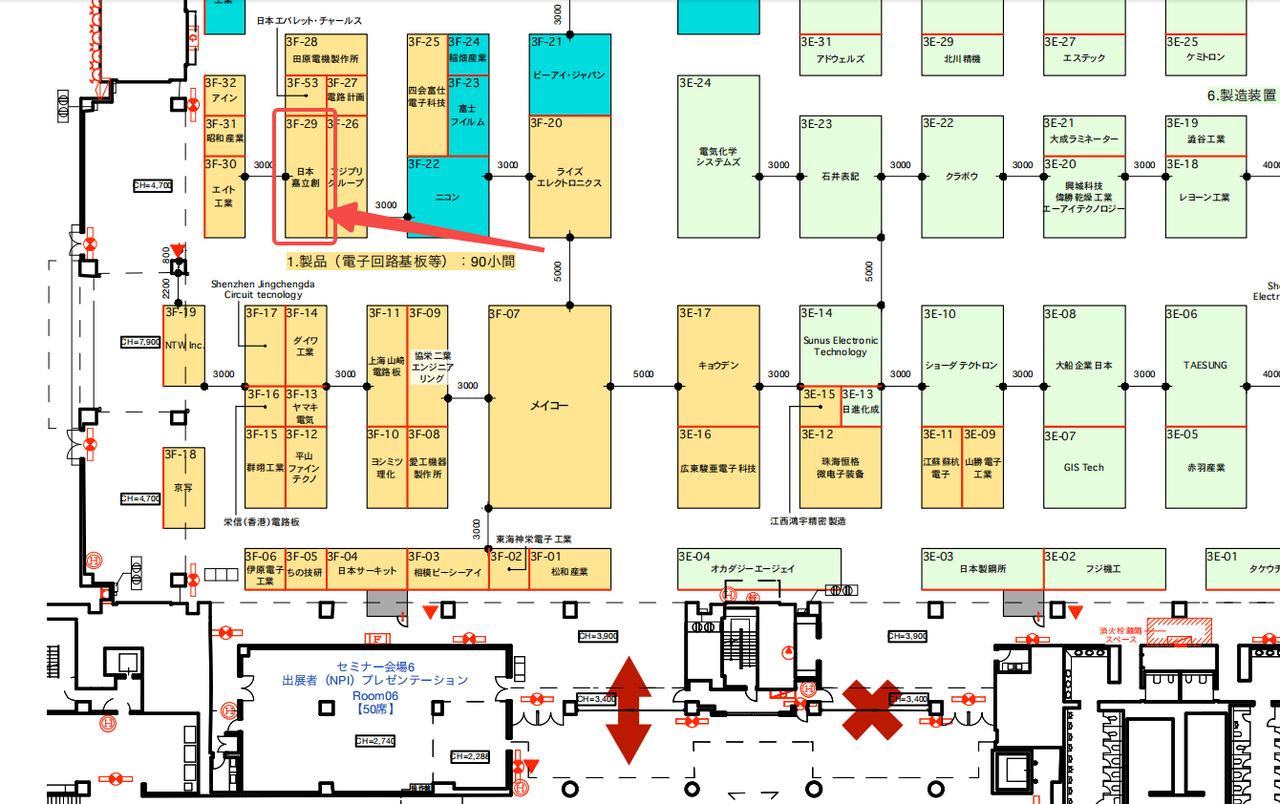
Location: Tokyo Big Sight, East Exhibition Halls, Japan
Booth Number: 3F-29
Dates: June 10 – 12, 2026
Exclusive On-Site Rewards
To celebrate opening day, we invite visitors to enjoy exclusive booth activities:
- JLCPCB Engineering Gifts: Engage with our team to claim limited-edition branded swag.
- $123 Welcome Coupons: Scan the on-site QR codes to instantly unlock a $123 coupon package for your next hardware project.
About JLCPCB
JLCPCB is a full-stack, professional electronic manufacturing platform that simplifies hardware innovation. Powered by a deeply integrated ecosystem of EDA software, 1.2 million square meters of automated manufacturing bases, global component sourcing, and 400+ advanced SMT lines. JLCPCB enforces rigorous quality controls (including 4-Wire Kelvin tests and full-stage AOI) to make electronics manufacturing more professional, efficient, and reliable.
Visit us at Booth 3F-29 today! Let’s build better hardware, faster.
Recent News
• Notice on the Implementation of the EU Tax Reform Effective July 2026
Jul 02, 2026
• JLCPCB Launches High-Precision Back Drilling Process to Enhance Signal Integrity for High-Frequency Designs
May 13, 2026
• Logistics Update: Shipping Service Adjustments in the Middle East Region
Mar 03, 2026
• JLCPCB Exhibits at NEPCON Japan: Premier Global Partner for High-Quality EMS
Jul 01, 2026
• 2026 New Year’s Day Holiday Notice
Dec 29, 2025