
JLCPCB Launches High-Precision Back Drilling Process to Enhance Signal Integrity for High-Frequency Designs
Press Release
May 13, 2026- Introduction
- Overcoming Technical Challenges: Eliminating the "Antenna Effect"
- Key Advantages: A Leap in Performance and Cost-Efficiency
- Technical Specifications & Design Guidelines
- Ordering & Lead Time
Introduction
As the global electronics industry rapidly evolves, the speed and frequency of digital signal transmission have reached unprecedented levels. In this context, Signal Integrity (SI) has emerged as a critical core technology for PCB design. To empower engineers in addressing high-frequency circuit challenges, JLCPCB is proud to announce the official launch of its Back Drilling process. This technology effectively removes redundant via stubs, ensuring a more stable and cleaner transmission environment for high-speed signals.
Overcoming Technical Challenges: Eliminating the "Antenna Effect"
In traditional multi-layer PCB designs, unused portions of copper in a via (known as "stubs") act like antennas at high frequencies. This creates signal radiation that causes interference—such as reflection, delay, and attenuation—to surrounding signals. In severe cases, this interference can compromise the entire system's operation.
JLCPCB’s back drilling process, also known as Controlled Depth Drilling (CDD), utilizes a secondary drilling method with precise depth control to remove these unnecessary copper stubs, eliminating their negative impact on signal integrity.
Key Advantages: A Leap in Performance and Cost-Efficiency
- Enhanced Signal Quality: Significantly reduces noise interference and drastically improves signal integrity.
- Reduced Manufacturing Costs: By enabling through-holes to function like blind or buried vias, it reduces reliance on expensive and complex via structures.
- Lowered Complexity: Facilitates high-efficiency interconnections while simplifying the overall manufacturing complexity of multi-layer boards.
Technical Specifications & Design Guidelines
JLCPCB maintains strict control over the precision of the back drilling process to ensure every board meets high-frequency design requirements:
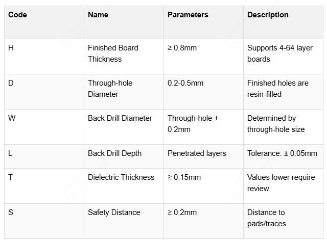
Important Note: A minimum clearance of 0.15mm must be maintained between the bottom of the back-drilled hole and the adjacent copper layer. All back-drilled holes are subsequently filled with resin, ensuring that the back-drilled portion is not visible in the final product.
Ordering & Lead Time
To ensure smooth production, please specify your back-drill requirements during the ordering process via one of the following methods:
- Separate Drill Files: Provide a separate file such as L1-2.drl (indicating back drilling from Layer 1 to 2).
- Distinct Diameters: Use different drill diameters to distinguish back-drilled vias (e.g., 0.31mm represents a specific back-drilled via).
Please Note: Back-drilled boards do not support expedited services; an additional 1-2 days must be added to the standard lead time.
Experience JLCPCB’s High-Precision Back Drilling Technology Today – Powering Your Next-Generation High-Frequency Designs!
Recent News
• Notice on the Implementation of the EU Tax Reform Effective July 2026
Jul 02, 2026
• JLCPCB Launches High-Precision Back Drilling Process to Enhance Signal Integrity for High-Frequency Designs
May 13, 2026
• Logistics Update: Shipping Service Adjustments in the Middle East Region
Mar 03, 2026
• JLCPCB Exhibits at NEPCON Japan: Premier Global Partner for High-Quality EMS
Jul 01, 2026
• 2026 New Year’s Day Holiday Notice
Dec 29, 2025