
Component Polarity & Orientation Identification Guide
Last updated on Jan 26, 2026
Definition of Polarity
Polarity refers to the correct alignment of a component’s positive/negative terminals or Pin 1 with the corresponding polarity markings or Pin 1 indication on the PCB (Printed Circuit Board). If the orientation of a component does not match the PCB markings, it is considered a reverse-polarity defect.
Throughout the PCBA process, polarity-related errors are critical. Incorrect orientation of polarized components may result in systematic failures, batch-level defects, or complete PCBA malfunction. Therefore, it is essential for engineering and production personnel to fully understand SMT component polarity rules. Polarity verification is also a key step in after-sales component failure analysis, to determine whether incorrect orientation caused PCBA failure or functional damage.
If you are using EasyEDA for PCB design or purchasing components through JLCPCB, polarity and orientation can often be quickly verified using the PCB footprint and schematic symbol libraries available on the JLCPCB / EasyEDA platform.
Common Polarized SMD Components
I. Capacitors
1. Tantalum Capacitors (Polarized Components)
On the physical component, the positive terminal is clearly marked. Common identification methods include:
- Color stripe
- “+” symbol
- Chamfered (beveled) edge
When designing PCB pads and silkscreen, clear polarity markings must be included.
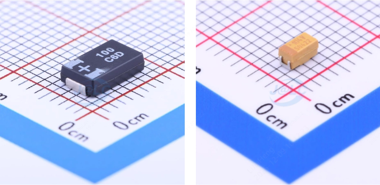
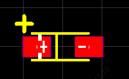
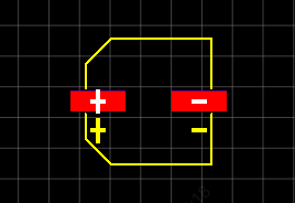
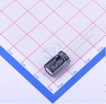
2. Aluminum Electrolytic Capacitors (Polarized Components)
a) SMD Type
For surface-mount electrolytic capacitors, the black band on the component body typically indicates the negative terminal.
Corresponding PCB footprint and silkscreen markings should reflect this polarity.

b) Through-Hole Type
For through-hole electrolytic capacitors, the negative terminal is usually marked with a white stripe or a stripe of a different color than the rest of the body.
The PCB footprint and silkscreen should clearly indicate polarity
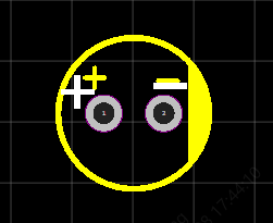
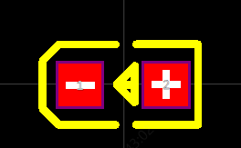
II. Light-Emitting Diodes (LEDs) – Polarized Components
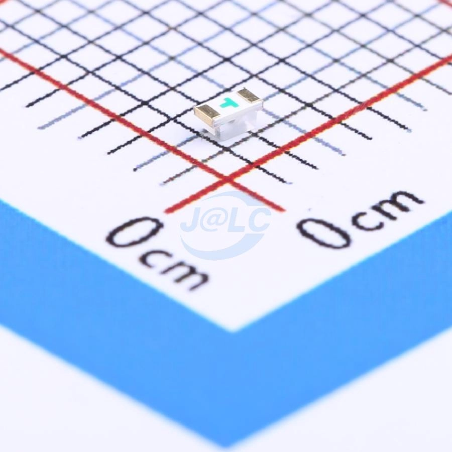
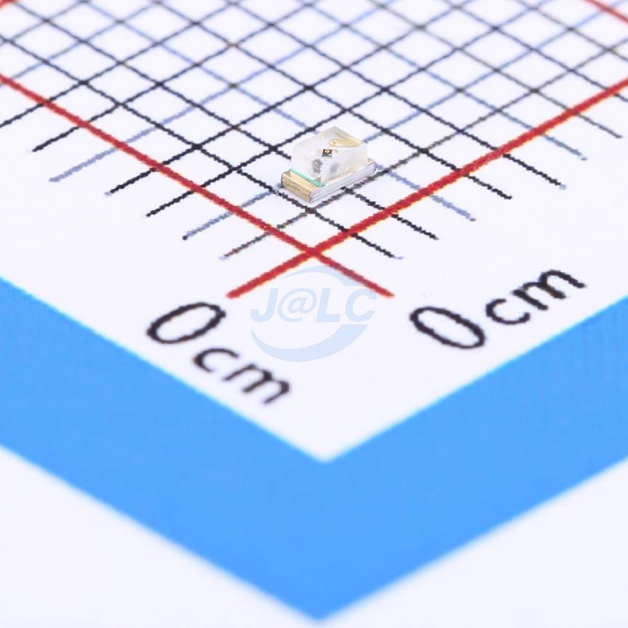
1. SMD LEDs
Polarity can be determined based on top-mount or bottom-mount orientation:
- When viewed from the top, the side with a green marking typically indicates the cathode (negative terminal).
- When viewed from the bottom, the arrow direction or raised arrow shape usually points to the cathode (negative terminal).
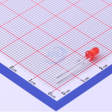
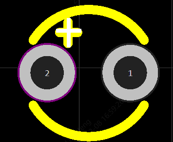
2. Through-Hole LEDs
- Before soldering, for two-lead LEDs, the longer lead is the anode (positive terminal).
- After soldering, polarity can usually be identified by distinct markings on the LED body, such as a white stripe.
III. Diodes – Polarized Components
For SMD diodes, the cathode (negative terminal) is typically indicated by:
- A color band
- A notch or groove
These markings should be visible on both the physical component and the PCB footprint.

IV. Integrated Circuits (ICs)
(Classification by Package Type)
IC polarity and orientation should be determined not only by the package marking, but also by cross-referencing the PCB silkscreen and pad layout.
During PCB design, it is essential to include clear silkscreen markings to enable unambiguous orientation verification.
It is generally recommended to place Pin 1 indicators outside the pad area or in an open board area for easy identification.
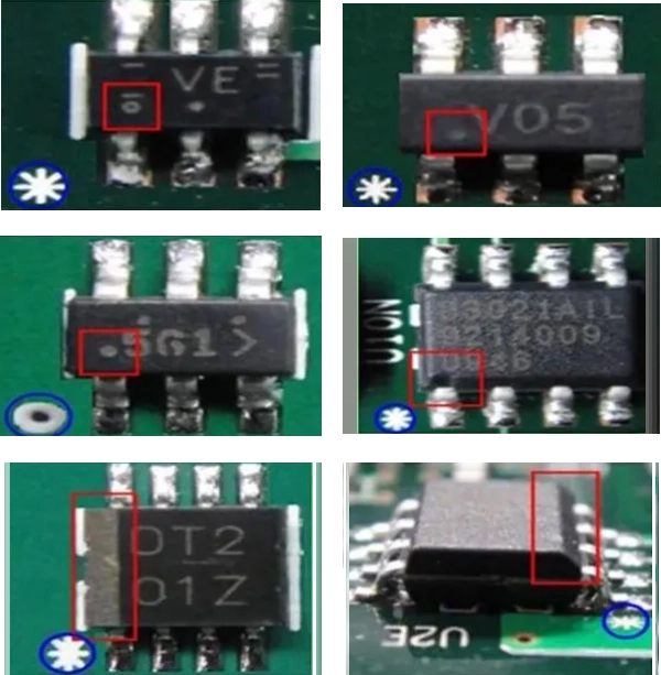
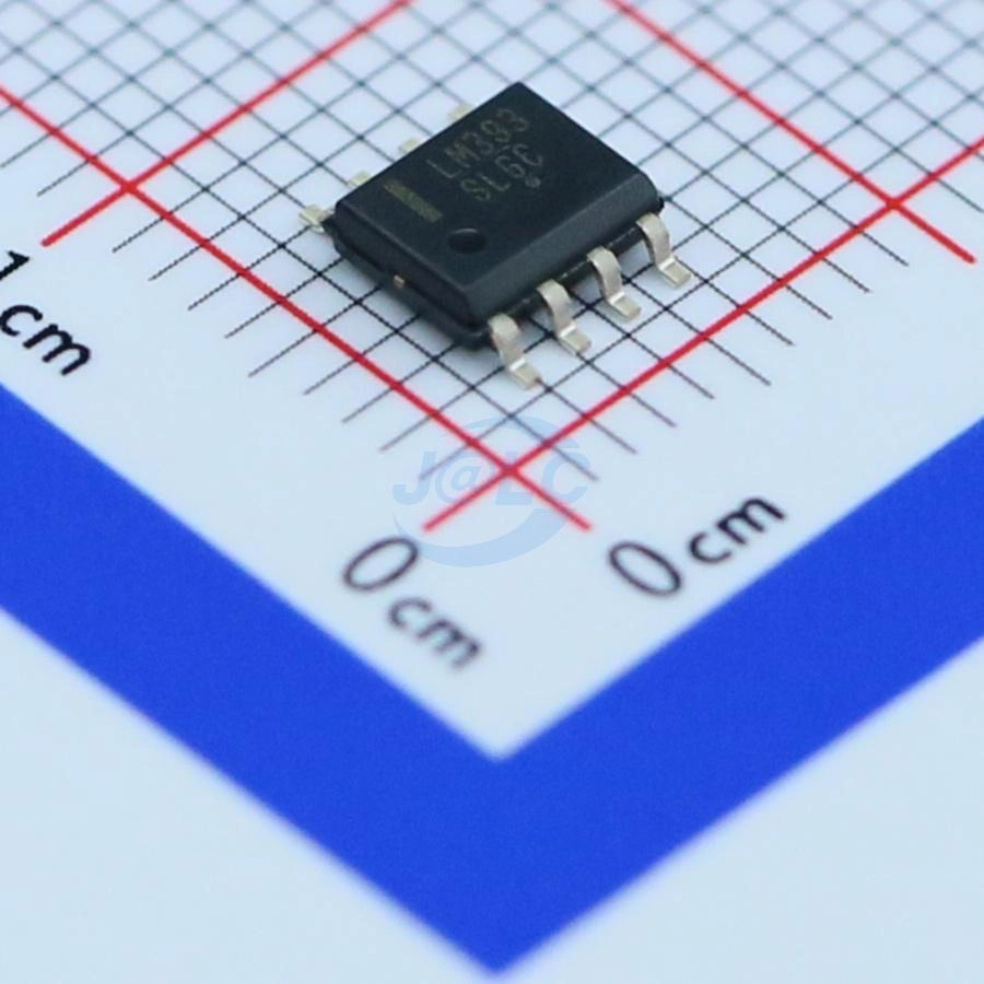
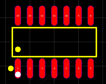
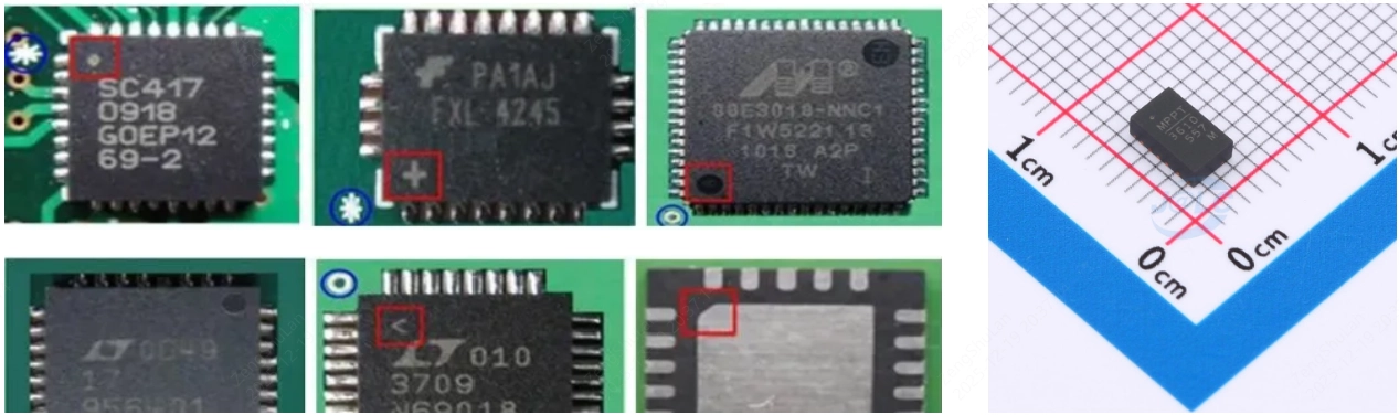
1. SOIC Packages
Pin 1 identification methods include:
- Color stripe
- Symbol marking
- Dimple or notch
- Chamfered edge
On the PCB footprint, Pin 1 is marked with a distinct and clear symbol near the corresponding pad.
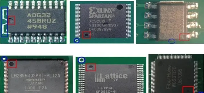
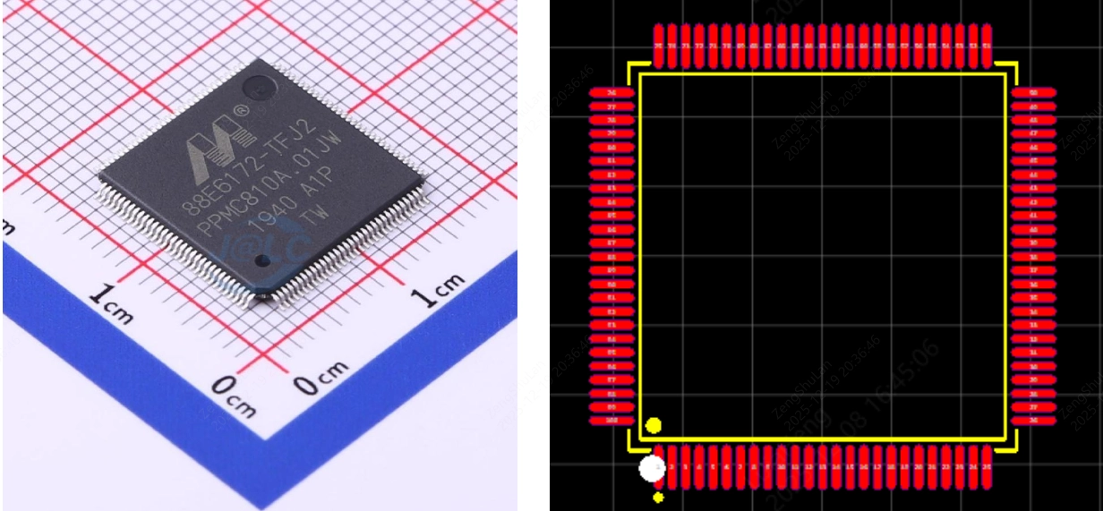
2. QFP / SOP Packages
These are square or rectangular packages with leads on all four sides.
Pin 1 is typically identified by:
- A dimple or notch
- One dot that differs from other dots in size or shape
The PCB footprint includes a distinct Pin 1 indicator near the corresponding pad.
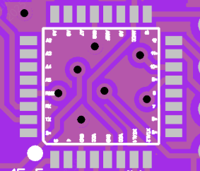
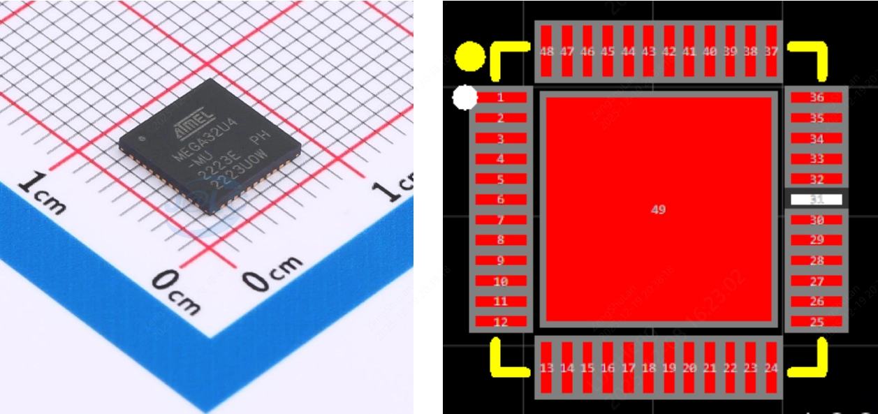
3. QFN Packages
- QFN packages with leads on two sides are typically rectangular.
- QFN packages with leads on all four sides are typically square.
Common Pin 1 indicators include:
- A dot that differs from other dots in size or shape
- A chamfered corner
- Symbol markings (e.g., line, “+” symbol, or dot)
The PCB footprint includes a clear and unique Pin 1 marking.
4. BGA Packages
In classic BGA packages, such as CPUs, the underside of the package is populated with an array of solder balls.
Polarity / Pin 1 identification is typically indicated by:
- Dimple or notch
- Dot or circular marking
The PCB footprint includes distinct Pin 1 indicators.

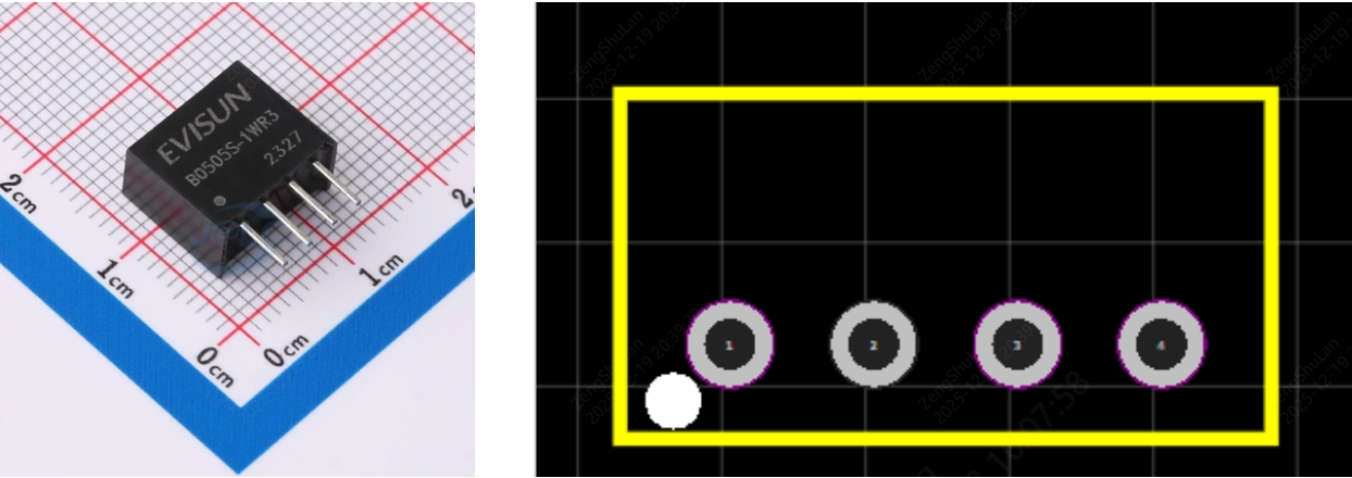
V. Power Modules
Many power modules include polarity or orientation indicators.
For through-hole power modules, common indicators include:
- Dimple or notch
- Dot or circular marking
On the PCB footprint, polarity is typically indicated by a circular marking or a square pad.
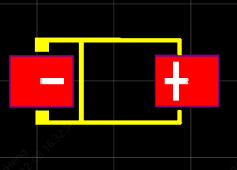
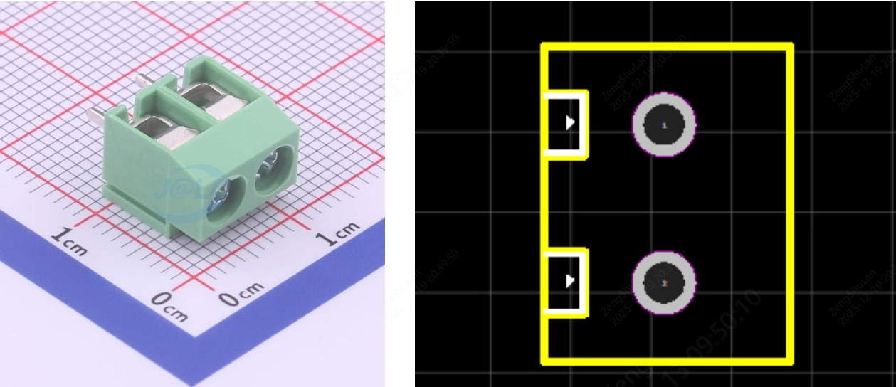
VI. Terminal Blocks / Connectors
Most terminal blocks do not have electrical polarity, but orientation during assembly is still critical, as it affects the alignment of external interfaces.
For these components, the footprint design typically includes directional indicators to ensure correct orientation during soldering and to avoid reversed connector installation.
Final Notes:
When verifying component polarity and orientation, always combine PCB silkscreen markings with physical component markings for confirmation. This dual verification approach helps ensure correct polarity and orientation, minimizing the risk of functional failure or irreversible damage.