Via-in-Pad Design Tutorial and Technical Guide
Last updated on Oct 16, 2026
Definition and Overview of Via-in-Pad
Via-in-pad, as the name suggests, refers to a plated via placed directly within a component pad, typically for surface-mount devices (SMDs) such as BGAs, QFNs, and LGAs. It is an increasingly common technique in modern high-density PCB design. Unlike traditional designs, where vias are placed beside component pads, via-in-pad places the via directly within the pad itself, offering significant space savings and performance benefits.
In simple terms, Via-in-Pad means placing the via on the pad itself, then during fabrication, using a resin/copper-paste plug plus electroplated cap process to manufacture it. This process greatly reduces the difficulty of fan-out routing for BGAs and other fine-pitch chips on high-density, compact boards.
As PCBs continue to evolve toward higher density and greater interconnectivity, there is less space available for routing traces and placing pads for conventional vias. This has led to the adoption of via-in-pad technology.
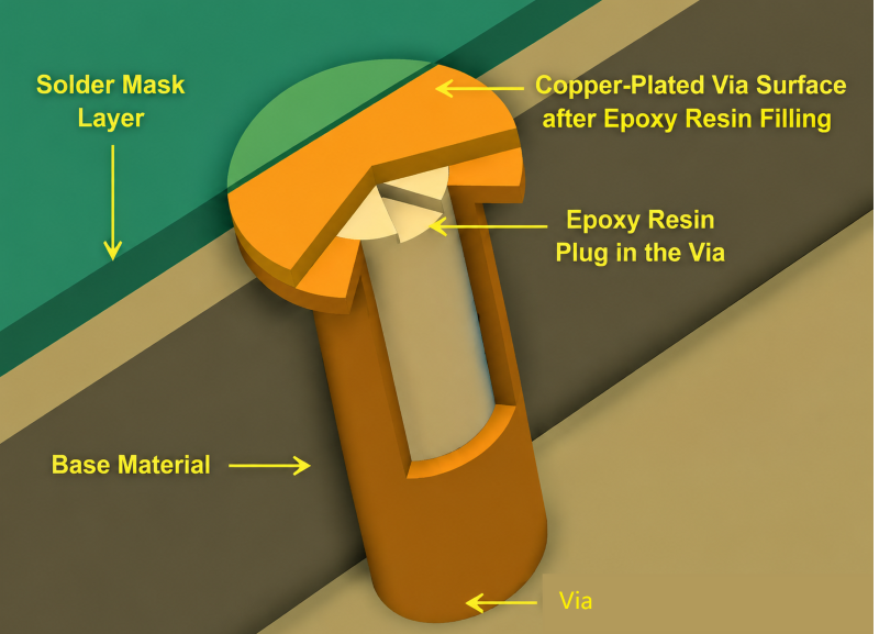
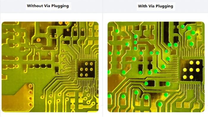
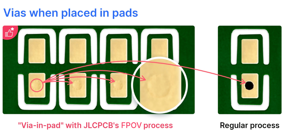
In simple terms, the process involves filling a plated via with a material such as insulating resin or conductive copper paste. The fill is then cured and planarized, followed by copper plating to create a flat surface. This allows the via to be covered with copper, leaving no visible opening on the PCB surface.
A 3D illustration of the via-in-pad process is shown below.
Via-in-Pad Dimensions
The dimension design of Via-in-Pad is a critical detail in PCB manufacturing, directly affecting solder joint reliability, signal integrity, and manufacturing cost. The key dimensional parameters and design guidelines are as follows:
Drill Diameter
- Typical recommendation: 0.15mm to 0.3mm (6mil to 12mil)
- Minimum capability: Laser drilling: 0.1mm (4mil); Mechanical drilling: 0.15mm (6mil)
Pad Diameter
- Minimum pad size = Drill diameter + 0.15mm (6mil)
Advantages of Via-in-Pad
Saves routing space and increases routing density:
- This is the key advantage of via-in-pad technology. In a traditional design, vias are placed beside component pads, requiring additional space for traces to connect the pads to the vias.
- Via-in-pad allows vias to be placed directly within the component pads, eliminating the need for these connecting traces and freeing up valuable routing space on the PCB surface and inner layers. This is particularly beneficial for fine-pitch packages such as BGAs, making it possible to accommodate more components and more complex interconnections within a limited board area.
Optimizes high-speed signal paths and improves signal integrity:
- Shortens signal return path: High-speed signals are very sensitive to path length. Via-in-Pad provides the shortest possible path from the component pad to inner-layer traces or power/ground planes, significantly reducing the parasitic inductance introduced by the via.
- Reduces signal reflection: A shorter path means fewer impedance discontinuities, helping to reduce signal reflections.
- Lowers crosstalk: More direct routing reduces the parallel length between signal traces, thereby lowering crosstalk risk.
- Improves power integrity: For power and ground pins, Via-in-Pad provides a very low-impedance current path to the inner power/ground planes, reducing voltage drop and power noise, and improving supply stability.
Improves thermal management:
For high-power components (such as CPUs, GPUs, and power ICs), copper-paste-filled Via-in-Pad under the ground or thermal pad can transfer heat more efficiently to the inner copper planes or the thermal layer on the back of the PCB, enhancing heat dissipation.
Reduces component footprint:
By eliminating the pad-to-via trace, component placement can theoretically be more compact, or more components can be placed in the same area (although actual placement is still subject to other design rules).
Simplifies layer count and routing design:
In extremely dense areas, Via-in-Pad can avoid complex escape routing and can also reduce the number of PCB layers, resulting in a cleaner design.
Application Scenarios
High-Density Interconnect (HDI) Design:
BGA packages: This is the most typical and primary application scenario. Modern BGA (Ball Grid Array) chips, especially those with very fine pitch (e.g., less than 0.8mm, commonly 0.5mm, 0.4mm or even smaller), have extremely limited space beneath the pads. The conventional peripheral via placement simply cannot accommodate the required number of vias to fan out all signals. Via-in-Pad allows vias to be placed directly beneath the BGA solder balls, fully utilizing the pad area itself, and is the only viable solution for connecting high-density BGA pins.
Fine-pitch components: In addition to BGA, other pin-dense packages such as certain QFN, LGA, and CSP packages, or multi-pin connectors, also require Via-in-Pad to meet routing needs when the pitch is very small.
Miniaturized devices: Products with extremely stringent space requirements, such as smartphones, tablets, wearables, drones, and high-performance computing cards, need to maximize every square inch of PCB area. Via-in-Pad is one of the key technologies enabling this level of miniaturization.
Improved Electrical Performance (especially high-speed / high-frequency circuits):
Shortens signal path: Via-in-Pad places the via directly beneath the pad, eliminating the short tracebetween the pad and the via in conventional designs. This significantly shortens the signal return path and reduces the overall signal path length.
Reduces inductance: A shorter path means lower parasitic inductance. This is critical for high-speed digital signals (such as DDR memory, high-speed SerDes lanes, PCIe, USB 3.0+) and RF/microwave signals, helping to reduce signal integrity issues (such as ringing, overshoot, and edge degradation) and electromagnetic interference (EMI).
Improves power integrity: For power/ground plane connections feeding BGA chips, Via-in-Pad provides a lower-impedance, more direct connection path. Multiple Via-in-Pad vias used in parallel (on larger power/ground pads) can significantly reduce the impedance of the power distribution network (PDN), reducing voltage fluctuation and noise.
Thermal Management:
Enhanced thermal conduction path: For power devices requiring good heat dissipation (such as CPUs, GPUs, power ICs, and LED driver chips), Via-in-Pad (typically filled with thermally conductive material) can transfer heat directly from beneath the device pad to the inner copper foil or the thermal layer/heatsink on the back of the PCB. This provides a more direct, lower thermal-resistance path compared to relying solely on the component body or surrounding copper pour.
Optimizes RF / Microwave Circuit Layout:
- Reduces discontinuities: In RF design, even minor impedance discontinuities can degrade performance. The conventional pad + peripheral via structure introduces a small impedance step between the pad and the via. The Via-in-Pad structure eliminates this extra pad-trace-via transition, providing a smoother path from the component pin to the transmission line and better impedance continuity.
- Reduces parasitic effects: Shorter paths help reduce parasitic capacitance and inductance, which is critical for impedance matching and performance in high-frequency circuits.
Challenges of Via-in-Pad
Solder Joint Reliability Risk (the biggest challenge):
Solder wicking: During reflow, molten solder may flow through the via to the back or inner layers of the PCB, resulting in insufficient solder at the joint (cold solder joint, voids), severely affecting connection reliability.
Solution: Resin plugging is the most commonly used and effective method. After the via is plated and filled, it is filled with insulating resin (typically epoxy) and cured, then ground flat. After resin plugging, the pad surface is flat, effectively preventing solder wicking, and surface finishes (such as ENIG, Immersion Tin, OSP) can be applied. Another method is full copper electroplating (the via is completely filled with copper), which is more expensive but offers better thermal and electrical conductivity and a flat surface.
Increased Manufacturing Cost
Via-in-pad often requires additional manufacturing steps, such as via filling and surface planarization, compared with standard through-hole fabrication. These processes add complexity and can increase PCB manufacturing costs and lead times, depending on the via structure and process requirements.
Design Complexity:
Via-in-Pad and its fill/plug requirements must be precisely configured in the PCB design software. Close communication with the PCB manufacturer is necessary to confirm their process capabilities and specifications (such as plug resin type, flatness requirements, minimum plug size, etc.).
Via-in-Pad Design Tutorial
Parameter Determination
Before placing Via-in-Pad vias, we need to first determine the BGA pad size, trace width, trace spacing, pad-to-pad pitch of the BGA, and the manufacturing process. This avoids overly large vias that result in insufficient spacing and inability to route out.
Here we set the trace width to 7mil (determine the actual trace width based on specific requirements, especially for special signals) and the trace spacing to 6mil. BGA pad size: 0.45mm. BGA pad-to-pad pitch: 1mm.
Via Size Determination
After determining the above parameters, you can begin setting the via size. For Via-in-Pad design, we need to consider the manufacturing capability of the PCB fab. Here we use the JLCPCB Via-in-Pad process design guide as the basis.
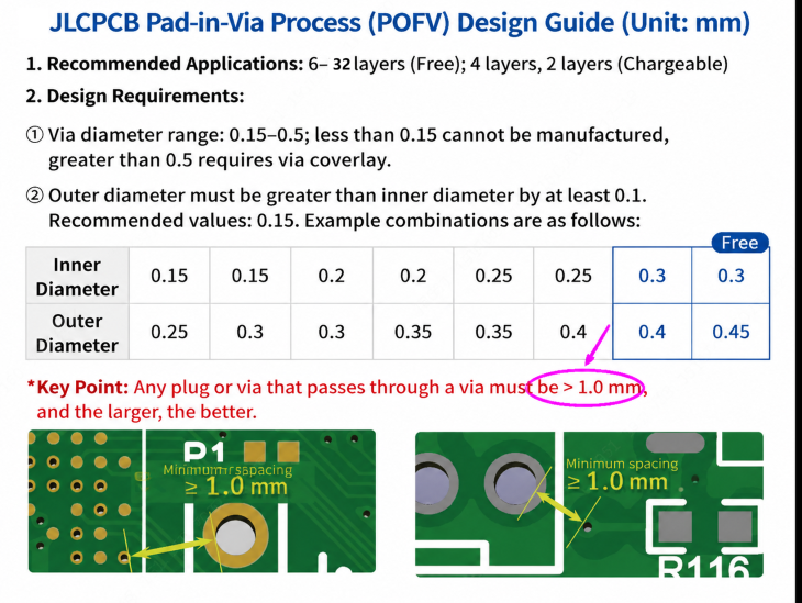
The BGA pad size is 0.45mm, so the via size must not exceed the pad size. Since we are using Via-in-Pad, the via can be set to the same size as the pad. Set the via outer diameter to 0.45mm (do not exceed the pad size). According to the recommendation, the inner diameter can be set to 0.3mm.
PCB Design
After setting the via parameters, you can begin placing Via-in-Pad vias. Via-in-Pad design is not as complicated as you might think; simply place the via on the pad. Before placing, remember to check the Properties panel on the right to verify that the via is set to Follow Rule and is using your configured size.
After configuration, you can begin placing vias onto the pads. The effect after placing Via-in-Pad is shown in the figures below.
Top layer overall fan-out routing:
Inner power plane 2 overall fan-out routing:
Inner power plane 4 overall fan-out routing:
Bottom layer overall fan-out routing:
PCB Ordering
After the design is complete, you can place an order directly in EasyEDA Professional Edition with one click.
For 6-layer or higher boards, JLCPCB will automatically select the corresponding process: Via Resin Plugged + Via Plated Capped with ENIG (Immersion Gold).
You can also see a PCB simulation render, which generates a 3D image based on the selected process options. Additionally, a free DFM check is available in the upper right corner.
Fabricated Board Photos
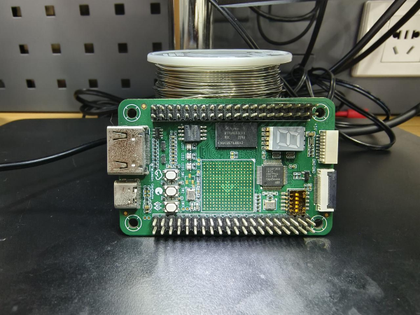
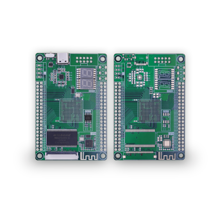
In the photos of the fabricated boards, you can see that the vias placed on the BGA have been covered. This is the JLCPCB Via-in-Pad process: Resin/Copper Paste Plug + Electroplated Cap.