How Is SMT Stencil Data Prepared for JLCPCB SMT Orders?
Last updated on May 16, 2026
JLCPCB operates an extensive component library and a well-established manufacturing process standard system. After customers submit SMT orders and design files, JLCPCB engineers generate optimized stencil aperture designs—either automatically or semi-automatically—based on the internal standardized stencil aperture rule database.
This ensures reliable solder paste deposition, component placement accuracy, and soldering consistency.
I. Workflow for Stencil Data Preparation
Stencil data is not generated directly from customer-provided Gerber files, but follows a standardized engineering workflow:
PCB Engineer: Creates the PCB fabrication data based on the Gerber files
⬇️
SMT Engineer: Generates the SMT production data based on the PCB fabrication data
⬇️
Stencil Engineer: Creates the stencil manufacturing files based on the verified single-board SMT data
This means that stencil production data is generated only after the SMT single-board verification is completed, rather than being derived directly from the customer’s original Gerber files.
Advantages of This Workflow
- The stencil design software is fully integrated with JLCPCB's internal systems
- The SMT engineering verification files contain complete package and pad information, enabling stencil engineers to clearly identify soldering locations
- This allows engineers to optimize stencil apertures based on engineering standards, improving solder joint consistency and long-term reliability rather than relying on raw pad geometry alone
II. Rules for SMT Stencil Data Generation
1. Stencil apertures are created only for SMT components. Through-hole (THT) components do not require stencil openings.
2. Only pads corresponding to components selected for placement in the order will receive stencil apertures and solder paste printing. Pads for components not selected for placement will not have stencil openings.
3. Stencil apertures are not identical to pad sizes. Engineers comprehensively evaluate:
- Component library data
- Industry-standard stencil design guidelines
- Component package types and pad structures
Based on these factors, stencil apertures are professionally optimized, rather than simply matching pad dimensions.
III. Preliminary Review of SMT Stencil Issues During the Customized Service Stage
(At this stage, production data has not yet been generated)
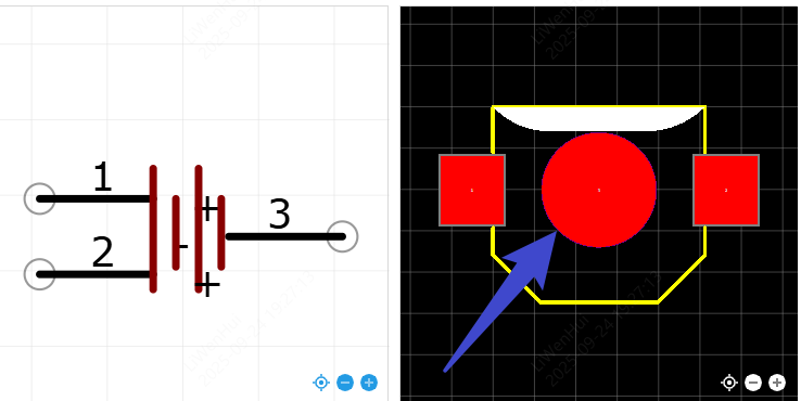
1. Battery Holder / Battery Socket Components
For battery-related components, whether the central circular pad requires a stencil aperture may vary depending on customer process requirements.
- During the customization review stage, if such components are detected, reviewers will proactively confirm with the customer whether the central circular pad requires an opening
- Due to system limitations, not all similar components can be automatically identified, and some may not trigger customer confirmation
To avoid order delays caused by confirmation requests, customers are strongly recommended to specify clearly in the order remarks whether stencil apertures are required for the central circular pads of such components.
If requirements are clearly stated in advance, engineers will apply the specified adjustments during the stencil preparation stage.
2. Precision Components
During the customization stage, the system first determines whether precision components are included in the order:
If included, customers will be consulted on whether to:
- Replace the component, or
- Use a step stencil
If the customer agrees to use a step stencil:
- The step stencil fee is charged first
- Final technical evaluation is performed by the stencil engineer after the order is successfully transferred to production
If the engineer later confirms that a step stencil is not required:
The step stencil fee will be refunded
3. Solder Paste Printing on Pads Without Component Placement (Special Stencil Apertures)
Stencil engineering only supports special apertures on the layer selected for placement in the order:
- Top-side placement selected → bottom-side special apertures not supported
- Bottom-side placement selected → top-side special apertures not supported
If solder paste printing is required on pads where no components are placed, the customer must clearly specify the exact locations so that special stencil apertures can be applied
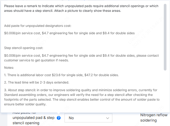
4. Customized Stencil Aperture Requests via Order Remarks
If customers have special soldering requirements (e.g., specific solder volume requirements for a particular BGA), they may:
- Add detailed remarks during order submission, or
- Contact customer support to add remarks on their behalf
Engineers will make corresponding adjustments before stencil data generation.
Important Note
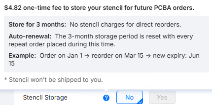
SMT stencils associated with SMT orders are not shipped.
However, stencil data can be stored for repeat orders, enabling consistent reproduction for future builds.