
What Inspection Capabilities Does JLCPCB's SMT Assembly Service Provide?
Last updated on Feb 02, 2026
In SMT assembly, inspection capability is a critical factor that directly determines the stability of soldering quality and the long-term reliability of PCBA products.
To ensure consistency and process controllability during mass production, JLCPCB has implemented multi-dimensional soldering quality inspection and testing measures throughout the entire SMT manufacturing flow.
These measures enable full-process monitoring of solder paste printing, component placement, and soldering results, allowing potential soldering risks to be identified and controlled at an early stage, and ensuring that delivered products consistently meet process specifications and customer requirements.
The following are the primary soldering quality inspection methods deployed in JLCPCB's SMT assembly process.
1. SPI (Solder Paste Inspection)
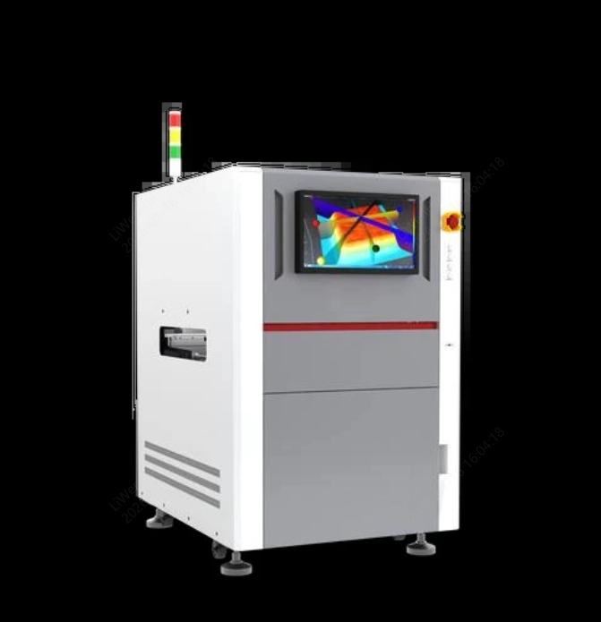
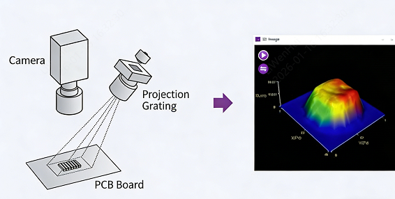
SPI (Solder Paste Inspection) is a core inspection system in SMT manufacturing used to control solder paste printing quality. JLCPCB utilizes 3D SPI systems to perform high-precision analysis of solder paste conditions after printing, providing a reliable quality foundation for subsequent placement and reflow soldering processes.
Inspection Position
SPI inspection is performed after solder paste printing and before component placement, serving as a front-end quality control step in the SMT process.
By inspecting solder paste conditions at this stage, potential defects can be detected before soldering occurs, preventing issues from propagating into downstream processes.
Inspection Scope
Using 3D SPI systems, JLCPCB conducts comprehensive inspection of the geometric characteristics of printed solder paste, including but not limited to:
- Solder paste volume
- Solder paste area
- Solder paste height
- X/Y positional offset
- Paste shape and edge collapse
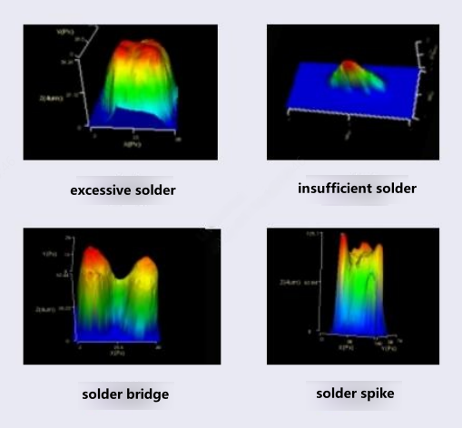
- Printing defects such as bridging, insufficient paste, excessive paste, and solder spikes
It should be noted that SPI focuses on the visual and geometric properties of solder paste. It does not evaluate the chemical characteristics of solder paste, such as flux activity, oxidation level, or wetting performance.
Value and Significance
In practical SMT production, the majority of soldering defects originate from abnormalities during the solder paste printing stage. As the starting point of the soldering process, solder paste printing directly determines the solder volume, position, and morphology, which in turn has a decisive impact on placement accuracy and reflow soldering results.
By performing SPI inspection prior to component placement and reflow soldering, potential risks such as insufficient paste, excessive paste, misalignment, and solder bridging can be identified in advance. Since downstream processes cannot correct printing-related defects, allowing such issues to pass through significantly increases rework difficulty and cost, and may even result in batch-level soldering failures.
For this reason, JLCPCB integrates SPI inspection immediately after solder paste printing to implement front-end quality control, effectively reducing the probability of soldering defects at the source and improving overall process yield.
2. AOI (Automated Optical Inspection)
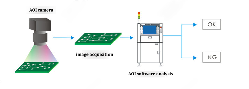
AOI (Automated Optical Inspection) is a core inspection system in SMT manufacturing, used to inspect component placement and soldering appearance quality. It is one of the most widely used and mature standardized inspection methods in the industry.
In SMT production, JLCPCB is equipped with 2D AOI and 3D AOI systems to conduct systematic and standardized inspections of placement and soldering results, ensuring that product appearance and assembly quality are controlled before entering the next process.
Inspection Position
AOI inspection is typically performed after SMT placement and after through-hole assembly, providing comprehensive visual inspection of completed PCBA assemblies.
By placing AOI inspection at critical process checkpoints, defective boards can be identified and isolated before proceeding to downstream operations, preventing defect amplification or escape.
Inspection Scope
AOI systems use high-resolution industrial cameras to scan PCB surfaces and compare captured images against reference data or process parameters. Key inspection items include:
- Missing, incorrect, or reversed components
- Component misalignment, skewing, and tombstoning
- Solder joint appearance defects such as insufficient solder, excessive solder, and solder bridging
2D AOI is mainly used for planar appearance and placement inspection, while 3D AOI further measures and analyzes solder joint height, volume, and three-dimensional profiles, providing higher recognition capability for fine-pitch components.
Through AOI application, high-coverage inspection of the entire PCB can be achieved, effectively identifying subtle defects that are easily missed by manual visual inspection.
Value and Significance
AOI offers advantages such as high inspection speed, excellent repeatability, and consistent judgment criteria, making it especially suitable for medium- to high-volume and stable mass production.
Compared with traditional manual inspection, AOI delivers the following benefits:
- Uniform inspection standards, minimizing subjective variation and operator fatigue
- High inspection efficiency, compatible with continuous production takt times
- Traceable inspection results, supporting quality analysis and continuous improvement
Through 2D and/or 3D AOI inspection, JLCPCB is able to promptly identify and intercept various placement and soldering appearance defects before products enter the next process, reduce the risk of defects flowing into downstream processes, effectively lower rework rates and customer defect occurrence probability, and ensure the stability of delivery quality.
3. Visual Inspection
Visual Inspection is a fundamental quality control method in SMT production, performed by trained and experienced inspectors who evaluate the appearance and soldering condition of PCBAs using direct visual observation, supplemented by necessary inspection aids.
Inspection Position
Visual inspection is typically conducted after SMT placement and after through-hole assembly, serving as a complementary checkpoint at key process stages.
It is used to verify automated inspection results and to manually review conditions that are difficult for inspection equipment to assess accurately.
Inspection Scope
Compared with automated inspection systems, manual visual inspection offers greater flexibility in certain scenarios and plays an effective supplementary role, particularly in the following areas:
- Irregular component structures, special layouts, or regions that are difficult for automated equipment to fully cover
- Rapid identification and verification of obvious visual abnormalities
- Direct confirmation of solder joint appearance and component polarity
- Customer-specified critical locations or special cosmetic requirements
Through human intervention, more targeted inspection can be applied to complex structures or customized requirements, improving the practical effectiveness of quality control.
Value and Significance
Visual inspection further reduces the risk of obvious appearance defects flowing into subsequent processes or reaching the customer, and is particularly suitable for low-volume production and products with complex mechanical structures.
It should be noted that manual visual inspection is primarily effective at identifying highly visible appearance defects. In terms of inspection consistency, detection of subtle soldering defects, and high-repeatability judgment, it cannot replace automated inspection systems such as AOI. For this reason, JLCPCB positions visual inspection as a supplementary and safeguard measure within the overall automated inspection framework.
By adopting a combined approach of “automated inspection + manual verification,” JLCPCB ensures inspection efficiency while effectively reducing false calls and missed defects, further improving overall inspection coverage and PCBA quality stability.
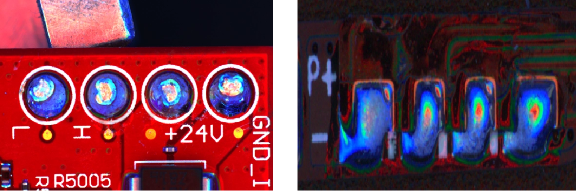
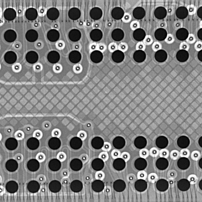
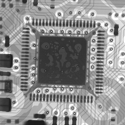
4. X-Ray Inspection
X-Ray inspection is a critical inspection method in SMT production used to evaluate the internal structural quality of solder joints. It is primarily applied to package types that cannot be effectively inspected by visual inspection or AOI, and serves as a key quality assurance process for high-density and high-reliability PCBA products.
Inspection Position
X-Ray inspection is typically performed after SMT assembly, allowing non-destructive internal inspection of fully soldered PCBAs to assess the actual condition of hidden solder joints.
Inspection Scope
X-Ray systems use X-ray penetration to image PCB and solder joint structures, enabling detailed analysis of solder joint morphology, solder distribution, and interconnections.
This inspection focuses on the “invisible” aspects of solder joint quality, including:
- Solder joint integrity and solder coverage
- Voiding within solder joints
- Bridging or misalignment of solder balls
- Internal soldering defects such as cold joints, non-wetting, or false solder joints
Value and Significance
As electronic products continue to trend toward miniaturization and higher integration, bottom-terminated components such as BGA, QFN, and LGA are increasingly adopted. For these packages, solder joints are completely hidden beneath the component body, making effective quality evaluation difficult using visual inspection and AOI alone.
X-Ray inspection specifically targets these non-visible bottom solder joints, enabling early detection of potential soldering risks during production and ensuring that soldering quality remains within controlled limits. While AOI focuses primarily on appearance and placement verification, X-Ray inspection emphasizes internal solder joint structure, effectively identifying hidden defects that cannot be detected by human vision or AOI systems.
This inspection method has been widely applied in industries such as industrial control, medical devices, and communications, where higher reliability and long-term stability are required. For products with stringent reliability requirements or high sensitivity to solder joint failure, JLCPCB incorporates X-Ray inspection to further enhance soldering quality control and delivery assurance, while also supporting improved quality traceability and root-cause analysis.
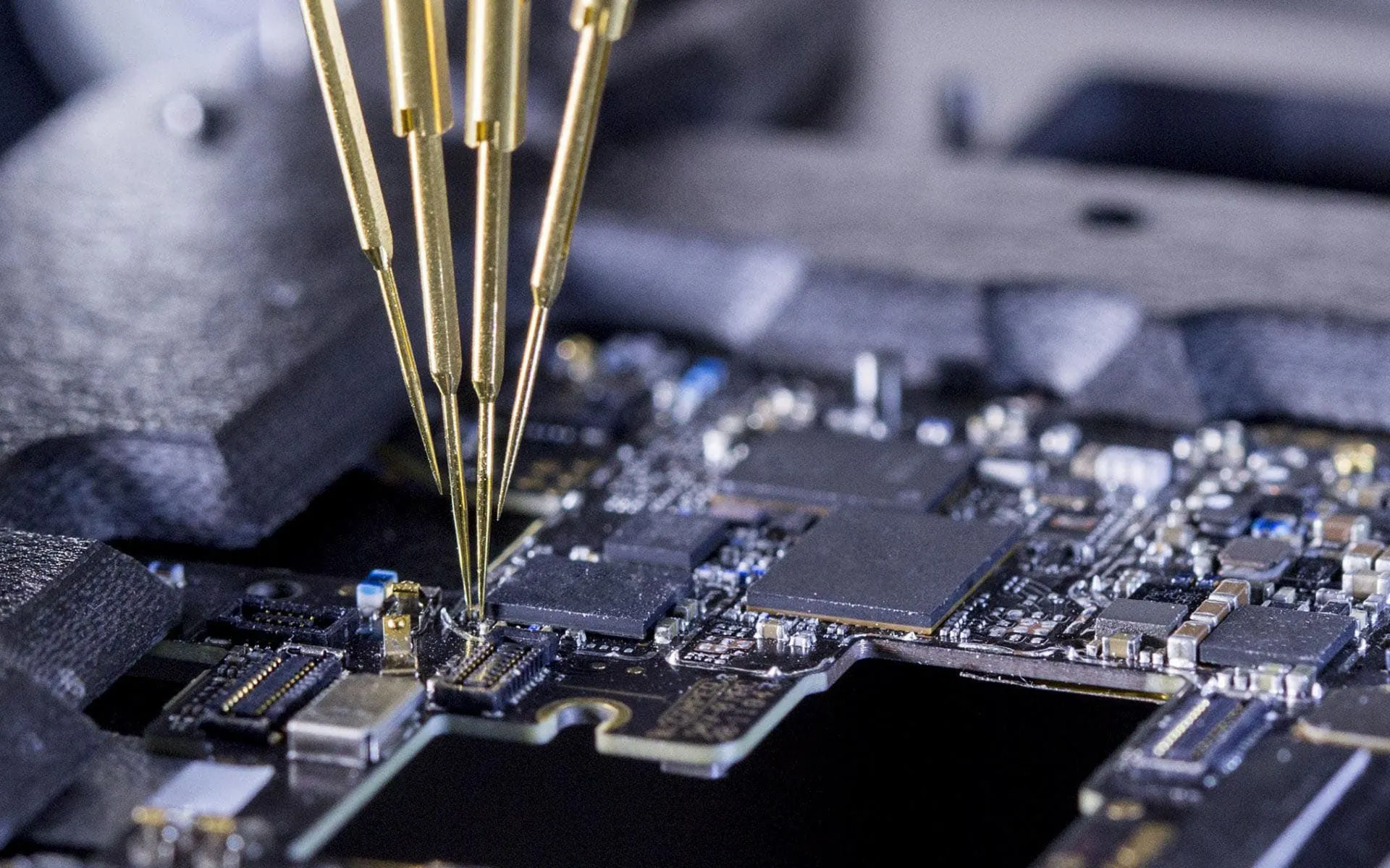
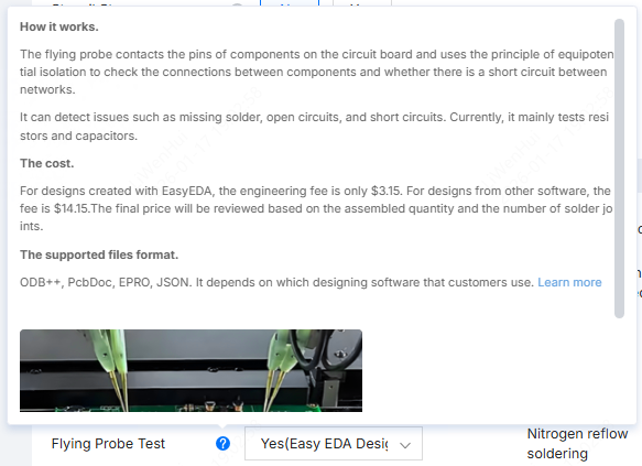
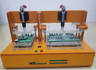
5. Flying Probe Test
The PCBA Flying Probe Test is an electrical test method that does not require dedicated test fixtures. During testing, multiple high-precision movable probe pins (“flying probes”) sequentially contact component pads or test points on the PCBA according to pre-programmed coordinate data, enabling point-by-point electrical verification.
It is a widely adopted testing approach in SMT production, particularly suitable for prototype, NPI, and low- to medium-volume manufacturing.
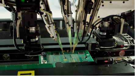
Test Position
Flying probe testing is typically performed after SMT placement and before through-hole assembly, i.e., after surface-mount components have been assembled and prior to the product entering subsequent processes.
At this stage, the test focuses on verifying the correctness and compliance of mounted SMT components before further value is added in downstream operations.
Test Scope
Flying probe testing evaluates PCBA electrical integrity through direct electrical contact, with primary test items including:
- Component value verification
Flying probes contact pads connected to both terminals of a component and apply specific voltage or signal stimuli to determine whether the measured component value meets design specifications.
- Open and short circuit detection
Test currents or voltages are applied between designated test points to identify open circuits or unintended short circuits.
- Component electrical characteristic testing
By contacting component leads, flying probes can verify electrical characteristics such as forward voltage, conduction state, and component polarity.
During the test process, flying probes directly contact component pads to evaluate component values, electrical characteristics, and net connectivity. Based on these results, the correctness of component placement, solder joint integrity at component leads, and overall component compliance on the PCBA can be assessed.
Value and Significance
- High cost-effectiveness
For low-volume or trial production, traditional functional circuit testing (FCT) typically requires custom fixtures, which involve high cost and long lead times and may impact overall delivery schedules. Flying probe testing eliminates the need for fixtures, enabling rapid test program deployment across different PCBA designs, significantly reducing test cost and shortening lead time.
- High test accuracy
Flying probe systems employ high-precision motion control and sensing technologies, enabling accurate probing of fine-pitch test points and ensuring stable, repeatable measurement results. The minimum supported component size can be as small as 0201 packages, with positioning accuracy reaching ±0.02 mm.
- High flexibility
Test programs can be flexibly adjusted during execution to quickly accommodate different product designs and customer-specific requirements, such as:
1. Defining probe keep-out zones or specified probing areas
2. Dynamically adding or modifying test items
3. Customizing test strategies based on product characteristics
Flying probe testing is positioned as a customized SMT test service. By incorporating flying probe testing into the SMT production process, JLCPCB can effectively control soldering quality and basic electrical reliability of PCBAs, helping customers identify potential risks early and improve overall product stability.
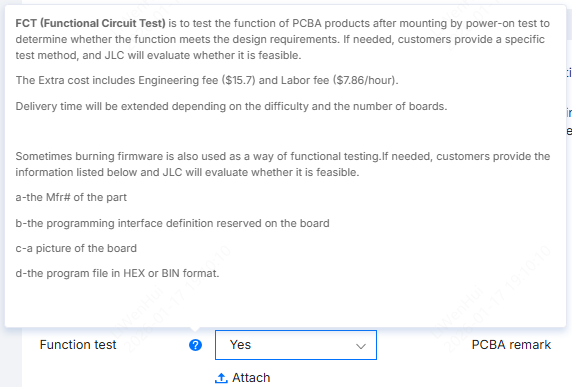
6. FCT (Functional Circuit Test)
FCT (Functional Circuit Test) is a critical testing method used during SMT production to verify whether the actual functional performance of a PCBA meets its design requirements.
Test Position
FCT is typically performed prior to shipment, serving as the final functional verification step before PCBA delivery. Its primary purpose is to intercept potential functional anomalies before products reach the customer, thereby reducing field application risks.
Test Scope
FCT is performed by powering on the fully assembled PCBA using a test fixture, dedicated test jig, or specialized test equipment to verify its functional performance.
During testing, the specific test methods and functional criteria are defined and provided by the customer based on product requirements. JLCPCB executes the tests strictly according to these specifications and delivers the corresponding test results.
Special Test Note: Firmware Programming
In certain application scenarios, firmware programming can be implemented as part of the functional test process.
By monitoring program execution status and validating critical checkpoints during firmware loading, basic functional verification of the PCBA can be achieved as part of the programming operation.
Value and Significance
Unlike inspection methods such as SPI, AOI, and X-Ray—which primarily focus on process control and soldering quality—FCT emphasizes functional validation under real operating conditions and serves as a key quality confirmation step prior to shipment.
Even when appearance inspection and soldering quality checks pass, functional abnormalities may still occur due to component defects, parameter deviations, or firmware-related issues during actual operation. As the final complement to upstream process inspection and soldering quality control, FCT enables functional-level validation of these potential risks before shipment, making it particularly suitable for products with high requirements for functional stability and reliability.
FCT is offered as a customized SMT service option, which customers can select when placing orders based on their specific needs. By introducing functional verification before shipment, JLCPCB can further confirm the actual operating status of PCBAs, effectively intercept potential functional failures, and enhance delivery consistency and reliability—providing a more stable foundation for customers’ downstream debugging and application.
Inspection System and Quality Assurance Overview
Through the combined application of SPI, AOI, X-Ray inspection, flying probe testing, and FCT, JLCPCB has established a comprehensive quality control system covering process monitoring, soldering verification, and functional validation throughout the SMT production lifecycle.
Each inspection and test stage serves a distinct role and works in coordination with the others to effectively intercept potential risks at different manufacturing phases, ensuring that PCBA soldering quality and delivery stability consistently meet customer requirements.
For details on supported personalized services and available options, please refer to our official Help Center documentation: https://jlcpcb.com/help/article/jlcpcb-supported-personalized-services