Help Center
Minimum Spacing Requirements for SMD Components
Last updated on Jun 12, 2026
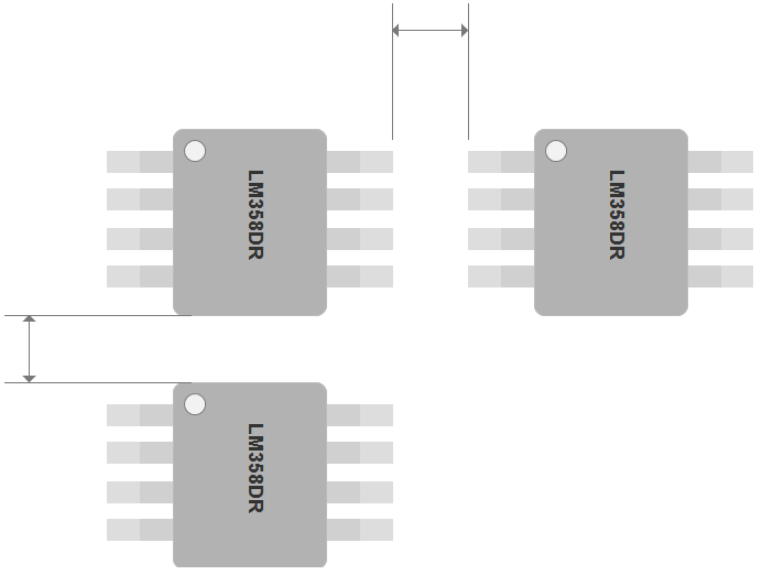
The values below represent JLCPCB's recommended minimum spacing requirements to ensure reliable SMT assembly, inspection, and rework accessibility.
These requirements are determined based on the following key manufacturing considerations:
- Component-to-component spacing between adjacent SMD components.
- Solder paste printing requirements and minimum stencil aperture separation.
- Inspection and rework accessibility, including AOI inspection and manual rework operations.
- Placement accuracy and tolerance of SMT pick-and-place equipment.
The table below lists the minimum recommended spacing requirements for commonly used SMD package types.
Note: Unit: mm[mil]
| Package | chip 0201 | chip 0402 | chip 0603 | chip 0805 | chip 1206 | QFN | QFP | SOP/ SOIC | SOT (SOT-23, SOT-363…) | BGA |
|---|---|---|---|---|---|---|---|---|---|---|
| chip 0201 | 0.15 [6] | 0.15 [6] | 0.18 [7] | 0.18 [7] | 0.25 [10] | 1 [40] | 0.5 [20] | 0.4 [16] | 0.2 [8] | 1.0 [40] |
| chip 0402 | 0.15 [6] | 0.18 [7] | 0.18 [7] | 0.25 [10] | 1 [40] | 0.5 [20] | 0.4 [16] | 0.2 [8] | 1.0 [40] | |
| chip 0603 | 0.18 [7] | 0.18 [7] | 0.25 [10] | 1 [40] | 0.5 [20] | 0.4 [16] | 0.2 [8] | 1.0 [40] | ||
| chip 0805 | 0.18 [7] | 0.25 [10] | 1 [40] | 0.5 [20] | 0.4 [16] | 0.2 [8] | 1.0 [40] | |||
| chip 1206 | 0.35 [14] | 1 [40] | 0.5 [20] | 0.4 [16] | 0.2 [8] | 1.0 [40] | ||||
| QFN | 1 [40] | 1.0 [40] | 1.0 [40] | 1.0 [40] | 1.5 [60] | |||||
| QFP | 1.25 [50] | 1.25 [50] | 1.0 [40] | 1.5 [60] | ||||||
| SOP/SOIC | 0.5 [20] | 0.4 [16] | 1.0 [40] | |||||||
| SOT (SOT-23, SOT-363…) | 0.4 [16] | 1.0 [40] | ||||||||
| BGA | 2.0 [80] |
SMD Component Spacing Measurement Method