
The Impact of Inner Layer Copper Coverage Rate on Board Thickness
Last updated on Mar 30, 2026
One of the most common material terms in the PCB manufacturing industry is prepreg, which is often referred to as being in the B-stage. These terms actually emphasize that this "adhesive sheet" between multilayer boards is in a special semi-cured state prior to lamination. It needs to flow as a liquid in a high-temperature pressing environment and fill the gaps between the boards within a limited pressing time. This process is also called "resin filling."
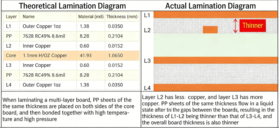
As can be easily deduced from the aforementioned concept, since the L2 layer has a very sparse distribution of copper patterns, when the prepreg flows in a liquid state under high temperature, high pressure, and high vacuum conditions, it will be directed to fill the various gaps between the layers. Because the area of the copper patterns on the L2 layer is smaller, there are more gaps to fill, which causes the overall thickness of the prepreg to be thinner after it cools and cures. If this type of deviation accumulates across multiple layers, it will cause the final board thickness to be too thin or even exceed tolerances.
Is there a way to improve or avoid this type of problem? This brings us to the concept of the "copper coverage rate."
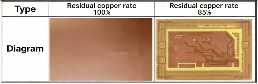
The copper coverage rate refers to the percentage of the entire board area occupied by the inner layer circuit patterns. Current layer copper coverage rate = Copper pattern area / Total area.
A brief overview of the multilayer board lamination process:
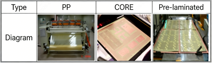
1. First, cut the prepreg into sheets that match the size of the working panel.
2. Prepare the prepreg, core boards, and copper foil according to the MI (Manufacturing Instructions) and lamination structure requirements.
3. After stacking, send the boards into a high-temperature, high-pressure vacuum press to melt the resin on the prepreg and fill the copper-free areas on the core board. After cooling, the resin cures, bonding the core board and copper foil together.
Obviously, for boards with an excessively low copper coverage rate, the overall manufactured board thickness will lean toward the thinner side. Additionally, the lack of copper pouring leads to an uneven copper distribution across the layers, making the board prone to warpage. Optimizing the pattern distribution during the design phase can fundamentally resolve this issue.


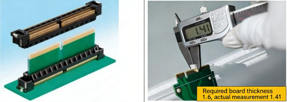
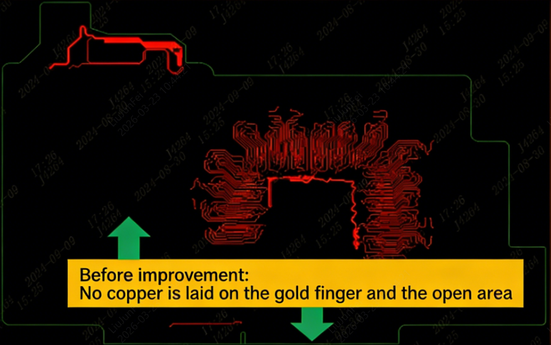
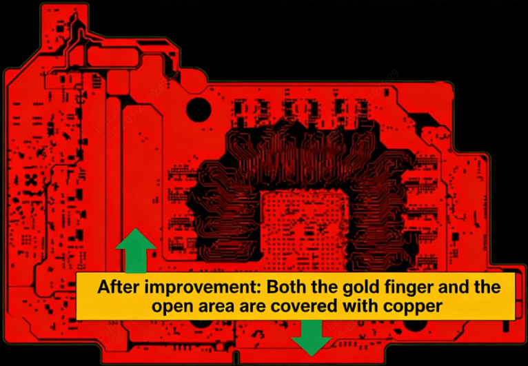
In addition, we need to specifically mention gold finger boards. Because gold finger boards need to be inserted into card slots, they are highly sensitive to thickness. A board that is too thin will result in a loose, unstable fit or poor electrical contact upon insertion.
Therefore, we strongly recommend:
1) For multilayer boards with gold fingers, apply a copper pour in the empty areas. In particular, the inner layers located at the gold finger area must have a copper pour to prevent the board from being too thin to fit securely into the slot, and to avoid defects such as uneven trace widths.
2) When the copper coverage rate is below 25%, please apply a copper pour in the empty areas to reduce uneven trace widths caused by inconsistent electroplating and to prevent excessive deviations in board thickness.
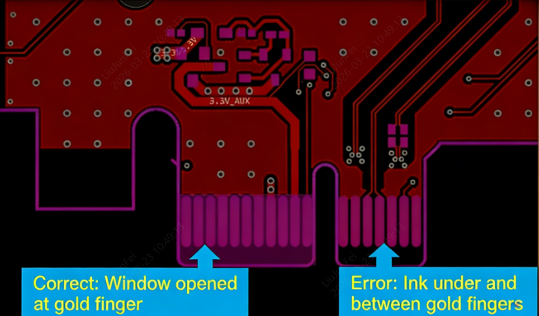
For the gold finger sections on the inner and outer layers, a full solder mask opening must be designed (i.e., there should be no solder mask bridges between individual gold finger pads). This prevents the solder mask from flaking off into the card slot during frequent insertion and extraction, which can cause functional issues like poor contact.
conclusion:
Regardless of the board type, as long as it does not affect the design's electrical performance, try to add copper pours to empty areas whenever possible. Copper pouring is absolutely essential, especially when the copper coverage rate is below 25%.
Furthermore, in gold finger designs, copper must be poured on the inner layers corresponding to the gold fingers. The solder mask opening for the outer layer gold fingers must ensure that no solder mask residue is left between the gold finger pads or at the front edge of the gold fingers.