
JLCPCB Launches Back Drill Process to Empower Faster and More Stable High-Frequency Signal
Last updated on Apr 23, 2026
As the electronic information industry evolves, the speed and frequency of digital signal transmission have reached new heights, making signal integrity (SI) a critical core technology.
Definition of Back Drilling
Traditional PCB designs often fail to meet the requirements of high-frequency circuits. When signal frequency increases to a certain threshold, the unused portion of copper in a PCB via acts like an antenna.
This creates signal radiation that causes interference—such as reflection, delay, and attenuation—to surrounding signals. In severe cases, this can compromise the entire system's operation.
Back drilling, also known as Controlled Depth Drilling (CDD), is used to remove these redundant copper stubs, eliminating their negative impact on signal integrity.
Advantages of Back Drilling
1. Reduces noise interference.
2. Improves signal integrity.
3. Reduces the reliance on blind and buried vias, thereby lowering PCB cost and manufacturing complexity.
Back Drilling Processing Method
Using a secondary drilling process with precise depth control, the unnecessary parts of a Plated Through Hole (PTH) are removed. For example, in a 6-layer board, if a signal only needs to connect the Top layer to Layer 2, a blind via would typically be required. With back drilling, a through-hole can be designed instead, and the copper plating from Layer 3 down to the Bottom layer is drilled away. This prevents the redundant copper stub from affecting signal integrity.
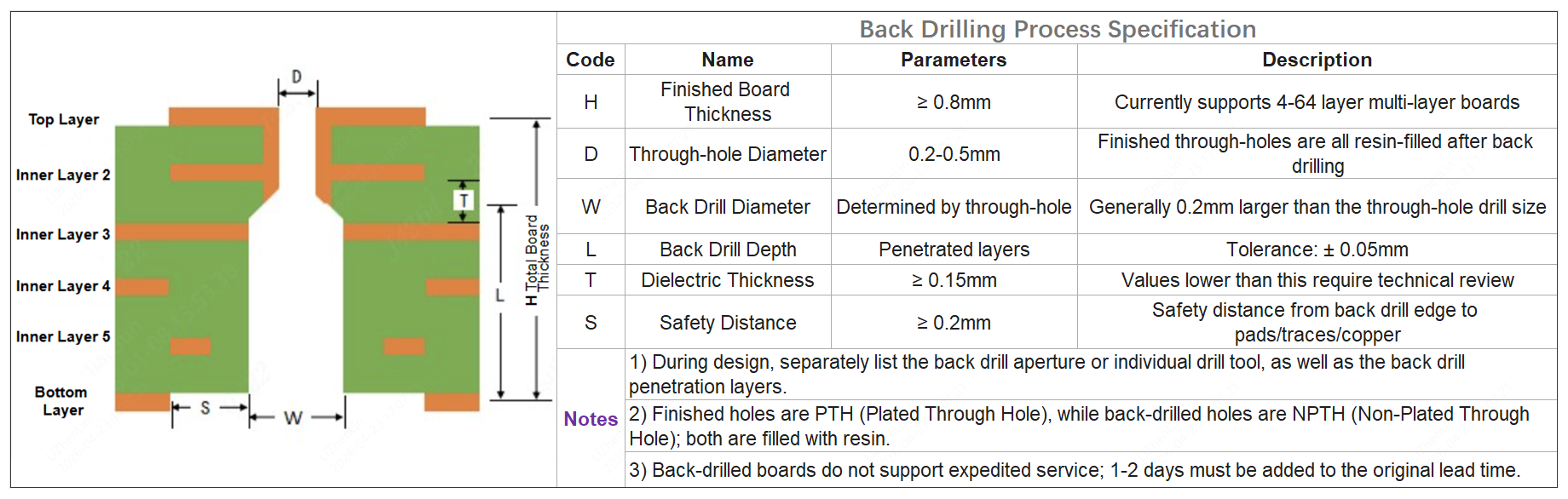
Important Technical Notes
1. Regardless of the layer count, vias intended for back drilling start as standard through-holes. These holes are drilled from the Top to the Bottom layer and then metallized via the copper plating process.
2. The purpose of back drilling is to remove the copper wall of specific layers. These holes are subsequently filled with resin, meaning the back-drilled portion is not visible in the final product.
3. A minimum clearance of 0.15mm must be maintained between the bottom of the back-drilled hole and the adjacent copper layer. Please verify your stack-up before designing the back-drill layers.
4. You can specify back-drill layers using two methods (please include a note during the ordering process):
(1): Provide a separate drill file for back drilling in addition to the standard through-hole drill file (e.g., L1-2.drl indicates back drilling from Layer 1 to 2; L1-3.drl indicates back drilling from Layer 1 to 3).
(2): Use different drill diameters to distinguish back-drilled vias (e.g., a 0.3mm hole represents a standard through-hole, 0.31mm represents a via back-drilled from Layer 1 to 2, and 0.32mm represents a via back-drilled from Layer 1 to 3).