6 Layer PCB Prototype & Stackup | JLCPCB
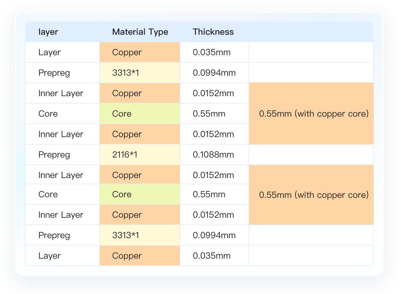
Typical 6 Layer PCB Stackup
A 6-layer PCB has 2 additional layers compared to standard 4 layer PCB. Typical 6-layer PCB stackup would be SIG/GND/PWR/SIG/GND/SIG. Power and ground layers are included for power management. This stacking technique reduces electromagnetic interference (EMI) and offers improved performance. 6-layer PCBs are commonly used in high-density applications, providing enhanced functionality and design flexibility.
Applications of 6 Layer PCBs
Devices with moderate ball count BGAs: 6-layer PCB’s are suitable for designs with multiple BGA’s and higher IO counts, providing sufficient routing capabilities for fine-pitch components.
High-power and high-speed digital/analog devices: 6-layer PCB's with dedicated power planes and signal layers support efficient power delivery and controlled impedance for demanding applications.
High-density designs with high-speed components: 6-layer PCB’s facilitate compact layouts with dedicated signal layers and power distribution, ensuring reliable performance for complex systems.
Mixed-signal PCB designs: 6-layer PCB’s allow for a dedicated analog section while accommodating high-density digital components and high-speed digital interfaces.

6 Layer PCB Capabilities
| Features | Capabilities |
|---|---|
| Max. Dimension | 660mm * 475mm |
| Dimension Tolerance | ±0.1mm(Precision) / ±0.2mm(Regular) for CNC routing, ±0.4mm for V-scoring |
| Board Thickness | 0.8/1.0/1.2/1.6/2.0 mm |
| Thickness Tolerance | ± 10%( Thickness≥1.0mm); ± 0.1mm(Thickness<1.0mm) |
| Controlled Impedance | |
| Via In Pad | Yes, free of charge, learn more > |
| TG | Tg 135-140 / Tg 155 |
| Minimum trace width and spacing | 3.5mil (0.09mm) |
| Min. Via hole size/diameter | 0.15mm / 0.25mm |
| Min. BGA Pad Dimensions | 0.25 mm |
| Drill Hole Size | 0.15mm - 6.30mm |
| Drill Hole Size Tolerance | +0.13/-0.08mm |
| Min. Pad Size | 1.0mm |
| Finished Outer Layer Copper | 1 oz / 2 oz (35um / 70um) |
| Finished Inner Layer Copper | 0.5 oz / 1 oz / 2 oz (17.5um / 35um / 70um) |
| Solder mask color | green, purple, red, yellow, blue, white, and black. |
| Surface Finish | ENIG (Free of charge) |
| Edge Plating | Yes |
The Benefits of JLCPCB 6 Layer PCB
 Free Via-in-Pad
JLCPCB offers free via-in-pad (VIP) technology for 6-layer PCB’s option.
Via-in-pad allows vias to be placed directly on the copper pads, resulting in increased design flexibility, less space requirement, enhanced thermal dissipation and improved electrical performance.
 Competitive Pricing
JLCPCB offers cost-effective pricing for 6-layer PCBs, ensuring affordability for customers without compromising on quality.
$0 for ENIG 2u'' surface finish and 5pcs 6-layer PCBs starts from $2.
 Fast Turnaround & Stable Quality
JLCPCB guarantees fast delivery with a turnaround time of as fast as 48 hours for 6-layer PCBs.Additionally, all orders go through a 4-wire Resistance Testing, ensuring consistent and reliable quality.
Frequently Asked Questions
- What is a 6 layer PCB?
A 6 layer PCB or printed circuit board is a type of PCB that consists of six conductive layers, sandwiched between insulating layers. With two additional layers, it provides more space for routing and reduced electromagnetic interference (EMI) compared to a standard 4 layer PCB.
- How thick is a 6 layer PCB?
The thickness of a 6 layer PCB can vary depending on the customer’s requirement or manufacturer’s specification. The Thickness of the 6-layer PCB ranges from 1.0 up to 2.0 millimeters, while the most commonly used is the 1.6mm option.
- What is the “via in pad” option for 6 layer PCBs?
The "via in pad" option for a 6-layer PCB refers to a PCB design technique where vias (plated holes) are placed directly within the pads of surface mount components. This allows for a more compact layout and improved routing efficiency. It's often used to optimize signal integrity and reduce signal distortion in high-speed electronic devices.
- What are the benefits of using 6 layer PCBs?
There are various benefits of using 6-layer PCB’s, however there are few crucial ones: Enhanced routing flexibility, Improved signal integrity as well as Higher component density.
- What is the typical 6 Layer PCB Stackup?
Typical 6-layer PCB stackup would be SIG/GND/PWR/SIG/GND/SIG. Power and ground layers are included for power management. This stacking technique reduces electromagnetic interference (EMI) and offers improved performance.
- What are the design rules for 6-layer PCB stack-up?
There are no standardized design rules for a 6-layer PCB stack-up as it can depend on various factors such as signal integrity requirements, manufacturing capabilities, and thermal considerations. However, before working on the PCB design, the initial step is to define design rules. At the same time, it’s a common rule to look at the manufacturer’s specification and use it to set the rules.
- How to do the material selection for 6 layer PCB’s?
Material selection for a 6-layer PCB involves considering factors such as electrical performance, thermal management, mechanical properties, manufacturability, and cost-effectiveness. By following and considering all relevant factors, you can make informed decisions about material selection for your 6-layer PCB design.
- What are the differences between a 6-layer PCB’s and a 4-layer PCB’s?
A 6-layer PCB is essentially a 4-layer board with 2 extra signal layers added between the planes. The 6-layer PCB standard stack-up includes 4 routing layers ( two outer layers and two internal layers) and 2 internal planes (one for ground and the other for power). This amplifies the EMI (Electromagnetic interference) considerably by offering 2 internal layers for high-speed signals and 2 external layers to route low-speed signals.
- How many layers of PCB do I need?
Determining the number of conductive layers required for your PCB involves considering factors such as the complexity of the design, signal integrity requirements, cost constraints, space limitations, thermal considerations, and the manufacturing capabilities of your chosen PCB manufacturer.
- What factors determine the purchase cost of a 6-layer PCB?
The purchase cost of a 6-layer PCB is determined by several different factors, such as PCB size, material selection, the complexity of design, manufacturing specifications (minimum clearances, minimum hole size), finish material, quantity, turnaround time, quality testing, etc…
- What are the power and signal layers in the PCB design?
In PCB design, power and signal layers refer to specific layers within the PCB stack up. Power layers carry electrical power to various components on the PCB. They typically consist of copper planes that distribute power throughout the board. Signal layers are used to route electrical signals between components on the PCB. They have traces that carry analog or digital signals.