
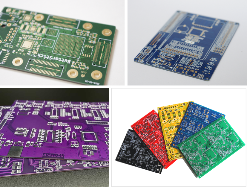
What is PCB Prototyping
PCB prototyping is the process of making a small-scale circuit board to test its functions before mass production. It helps designers and engineers validate and fine-tune designs for efficiency and accuracy. PCB prototyping allows for the identification and rectification of potential issues early in the design process, ultimately saving time and costs during full-scale production.
Why Choose JLCPCB for PCB Prototyping
 Fast Turnaround:
 Thanks to the smart technologies and fully automatic equipments, JLCPCB makes PCB prototypes as fast as in 24 hours. (5pcs for 1-4 layers) Customers have commended that the process is even faster than dealing with local suppliers.
 Top Quality:
 JLCPCB consistently focuses on the quality of PCB prototyping. Our engineering team will thoroughly review your files beofre production; we partner with top suppliers for raw materials and invests on advanced automatic machines.
 Good Value for Money:
 Large-scale and automated production assit JLCPCB in accelerating high production efficiency and reducing labor cost. Prices start at $2 for 1~8 layers and support up to 32 layers.
Frequently Asked Questions
- 1. How long can I get my PCB Prototypes?
The time for each order includes file review time, PCB production time, and delivery time. Generally, file review may take 1 to 2 days. Our quick turnaround PCB prototyping can be completed within 24 hours, but the time varies for different materials. For more details, see here:https://jlcpcb.com/help/article/PCB-Fabrication-Services-and-Production-Time The specific delivery time can be found on the quote page when selecting different couriers.
- 2. What raw materials JLCPCB use?
JLCPCB has always been partnering with top suppliers. We use top-level materials, like Nanya FR4 material, Solder mask with TAIYO INK PSR-2000; Lead-Free HASL-Rosh surface finish using upgraded raw materials which contain tin bars with silver.
- 3. What are the automatic equipment for JLCPCB PCB prototypes?
JLCPCB constants investments in advanced equipments including: Fully-automatic LDI exposure Machines. Fully-automatic Solder mask Production lines. Fully-automatic PCB Test Machines. Fully-automatic CCD exposure Machines. Fully-automatic PCB Etching Equipment. Fully-automatic Screen-printing Production lines. Fully-automatic Electroplating lines.
- 4. What is the minimum of PCBs I can prototype with JLCPCB?
We provide PCB prototyping starting by a 5pcs. 1~8Layer PCB for 5pcs just start from $2.
Your Premier Choice for PCB Prototype.
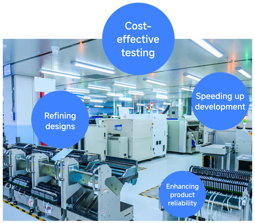
Benefits of PCB Prototyping
Cost-effective testing: PCB prototyping reduces rework, saving time and resources by detecting errors early, preventing costly modifications in later production phases.
Speeding up development: PCB prototype provides visual assistance and tangible models for evaluation. This visual aid helps engineers and designers identify issues more quickly, accelerating the design process.
Refining designs: PCB prototypes are vital for optimizing functionality, accuracy, and efficiency. Through iterative testing, designers refine circuits for peak performance, ensuring a reliable end product.
Enhancing product reliability: Through meticulous testing and refinement of PCB prototypes, the final product is more dependable and less prone to faults, ensuring a higher level of reliability.
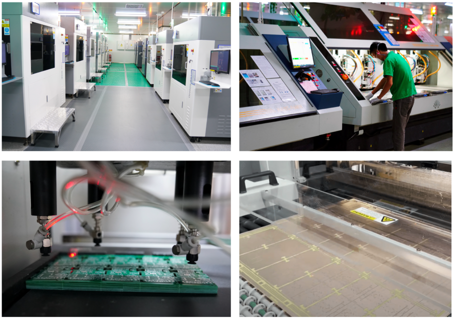
PCB Prototyping Process
Designing your circuit boards, creating Gerber files, and uploading to JLCPCB, the PCB prototyping process involves milling raw material into panels, followed by inner layer AOI(Automated Optical Inspection), drilling, copper plating, electro-etching, outer layer AOI, solder mask, silkscreen, and surface finishing. Concluding with AVI (Automatic Visual Inspection), VCUT, cleaning, QC checks, packaging, printing, and shipping, these steps ensure the quality and reliability of the final product.
PCB Prototyping
JLCPCB offers premium PCB prototyping services with a build time of 24 hours to realize your electronic ideas. Our PCB prototyping solutions satisfy the needs of engineers, designers, and manufacturers all over with prices starting at only $2.
$6
PCB Coupon
Valid for 30 days