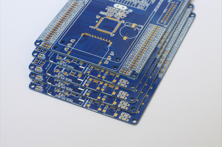
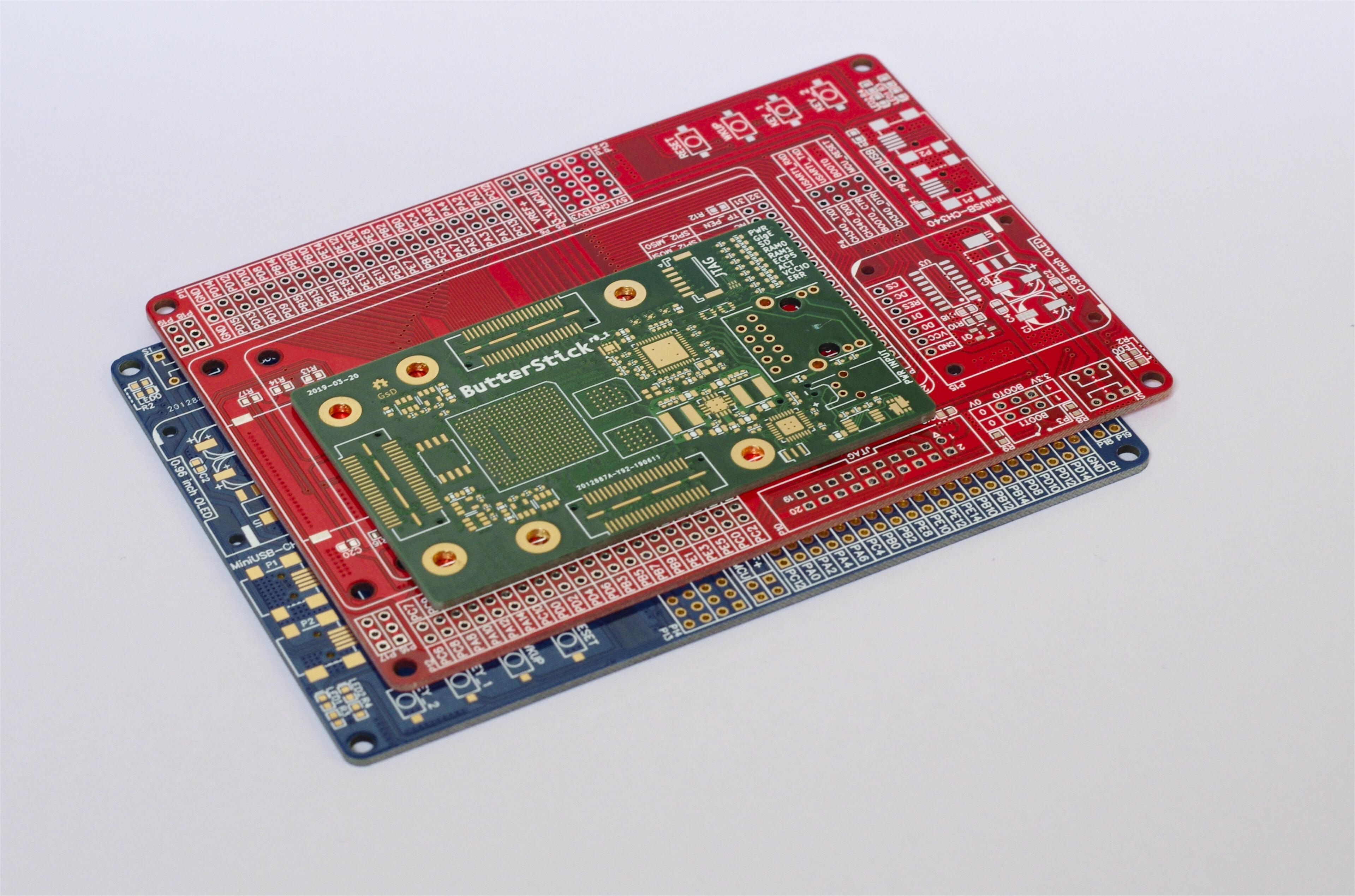
PCB Layers
JLCPCB offers a wide range of PCB layers, including our premium 6-layer PCB designed to meet your exact needs! Experience ultra fast 48-hour delivery and unbeatable pricing starting at just $2. Get your high-quality PCBs today.
$6
PCB Coupon
Valid for 30 days
What is a PCB Layer?
A PCB layer refers to the number of insulated copper layers in a PCB. Each layer serves a specific role in routing electrical signals and power between components. To establish an electrical connection between two components on a PCB, we need a copper trace, which creates a conductive path between components. Now, this conductive path runs through a single plane or multiple planes depending on the design complexity, and this conductive plane is basically a PCB layer. PCB ensures reliable electrical connections, while PCB layers enhance signal integrity, power distribution, and compact design for efficient circuit performance.
Types of PCB Layers
1-Layer PCB (Single-Sided PCB): One copper layer on an insulated PCB board. Application: Simple circuits like LED control, Logic gates, power regulators, etc.
2-Layer PCB (Double-Sided PCB): Copper layers on both sides of the PCB with vias for interconnections. Application: Microcontroller circuits, IOT devices, power control circuits, etc.
Multilayer PCB: PCBs that have more than two layers are called Multilayer PCBs. Two or more inner layers for power, ground, and signals for high signal reliability and integrity, which also improve EMI shielding and performance of PCB. Application: Industrial automation, medical devices, Smart devices, Aerospace devices, circuits for noisy environments, etc.
How to determine how many layers I need?
To determine the number of PCB layers needed, consider circuit complexity, signal integrity, and space constraints For simple circuits, where only a few components need connections, copper traces can lay on a single layer of the PCB, so we will choose to design a single-layer PCB. But when a circuit gets complex, with multiple components and high-speed signals, we will go for a multi-layer PCB, with separate layers for GND, POWER, HIGH-SPEED SIGNALS, etc. In this way, our PCB will work efficiently and provide reliable performance for a long life.
Advantages of JLCPCB Layers
 Premium Materials
 JLCPCB uses high-quality materials, like FR4 with a Tg of 140°C, ensuring robust performance and longevity in various applications.
 Competitive Pricing
 Offering 6-layer, 50x50mm boards with ENIG 2u" surface finish starting at just $2 for 5 pieces, JLCPCB provides affordable options without compromising quality.
 Fast Turnaround
 With a 48-hour turnaround time for multilayer PCBs and rigorous 4-wire resistance testing, JLCPCB ensures quick delivery and reliable performance for all projects.
Get Your Premium PCBs!
Frequently Asked Questions
- 1. What is a PCB layer, and why is it important?
A PCB layer refers to the number of insulated copper layers in a PCB. More layers improve signal integrity, power distribution, and space efficiency, making the circuit more reliable.
- 2. How do I decide how many PCB layers I need?
For simple circuits, a single-layer PCB is sufficient. For complex designs with multiple components and high-speed signals, a multi-layer PCB (2, 4, or 6 layers) is recommended.
- 3. What are the applications of different PCB layers?
1-layer PCB: LED control, logic gates. 2-layer PCB: IoT devices, power control circuits. 4-layer PCB: Industrial automation, medical devices. 6-layer PCB: Smartphones, aerospace electronics, high-speed circuits.
- 4. What are the advantages of JLCPCB's multi-layer PCBs?
JLCPCB offers high-quality materials (FR4 Tg 140°C), competitive pricing ($2 for 6-layer boards), and fast 48-hour turnaround with rigorous testing for reliability. We also offer free via-in-pad (VIP) technology for 6-layer PCB's option: https://jlcpcb.com/6-layer-pcb
- 5. How long does JLCPCB take to manufacture and deliver PCBs?
JLCPCB ensures 48-hour fast manufacturing for multi-layer PCBs, delivering high-quality boards quickly to meet project deadlines.