
Multiple Layer PCB
JLCPCB offers high-quality multi-layer PCBs (6-32 layers) with innovative Via-in-Pad (POFV) technology. POFV guarantees superior stability and reliability compared to traditional tented and plugged vias, featuring copper plating up to 25μm thick. Enjoy exceptional routing speed and heat management. Get started with a 6-layer PCB for just $2!
$30
6 Layer PCB Coupon
Valid for 60 days
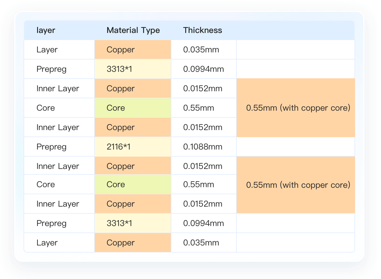
Typical Multiple Layer PCB Stackup
A multiple-layer PCB has at least three conducting layers and some insulating material in between them. The stack-up arrangement changes depending on the design needs. Each layer has its own job to do. Power and ground planes help control power distribution and lower electromagnetic interference (EMI). A typical stackup might look like this: (Signal/Ground/Power/Signal/Ground/Signal). Up to 32 layers are available on JLCPCB, which lets you make complicated designs with better signal integrity and better heat dissipation.

Applications of Multiple Layer PCBs
High-Density Consumer Electronics: Multilayer PCBs are an important part of smartphones, laptops, and wearable tech. The extra layers make routing and power control work well in small spaces.
Telecommunications Equipment: Multilayer printed circuit boards (PCBs) increase the reliability of signals and power transfer in network routers, 5G base stations, and signal processors. These boards make sure that gadgets that deal with high-frequency signals work reliably.
Medical Devices: X-ray machines and heart monitors are two examples of diagnostic tools that use layered PCBs to get low EMI and accurate performance. This makes sure that patient care is accurate and reliable.
IoT Devices and Smart Systems: Multilayer PCBs are perfect for connected devices because they allow for dense component placement and smooth data transfer. This makes them perfect for everything from smart home appliances to industrial IoT systems.
The Benefits of JLCPCB Multiple Layer PCB
 Free Via-in-Pad
 JLCPCB's POFV (Plated Over Filled Via) technology enhances PCB design flexibility with in-pad via placement, improves electrical performance through shorter traces, and ensures superior reliability with corrosion protection. Now free for 6-32 layer PCBs, JLCPCB makes advanced manufacturing accessible to all.
 Competitive Pricing
 JLCPCB offers competitive pricing on multilayer PCBs, with special promotions for cost-effective solutions. A 6-layer, 50x50mm board with ENIG 2u" surface finish starts at just $2 (for 5 pcs), and larger sizes such as the 6-layer 100x100mm boards begin at $35.1 (5 pcs).
 Fast Turnaround & Stable Quality
 JLCPCB promises fast shipping, and for multilayer PCBs, the turn-around time is as little as 48 hours. Each multilayer PCB undergoes rigorous 4-wire resistance testing to ensure consistent quality and reliability.
Frequently Asked Questions
- What is a multiple layer PCB?
A multiple-layer PCB is a type of printed circuit board with three or more conductive layers arranged among insulating materials. Complex circuit designs are better handled on it than single- or double-layer boards.
- How thick is a typical multiple layer PCB?
With 1.6 mm being the most usually used thickness for daily use, more than one layer of a printed circuit board can be any thickness between 1.0 mm and 2.0 mm.
- What advantages do multiple layer PCBs provide?
Multiple-layer printed circuit boards (PCBs) are ideal because they provide more route options, higher signal integrity, and more components per square inch, all of which are important for high-performance electronics.
- What is the typical stack-up for a multiple layer PCB?
Common stackup for a six-layer PCB is Signal/Ground/Power/Signal/Ground/Signal. This manages power flow and electromagnetic interference (EMI) rather well.
- How can I determine the number of layers needed for my PCB?
Before you decide on your design, consider the several layers your PCB requires depending on its design complexity, signal integrity needs, space constraints, and manufacturing capabilities.