
SMT Service Lead Time Overview
Last updated on May 16, 2026
1. Core Principle: How Is the Lead Time Calculated?
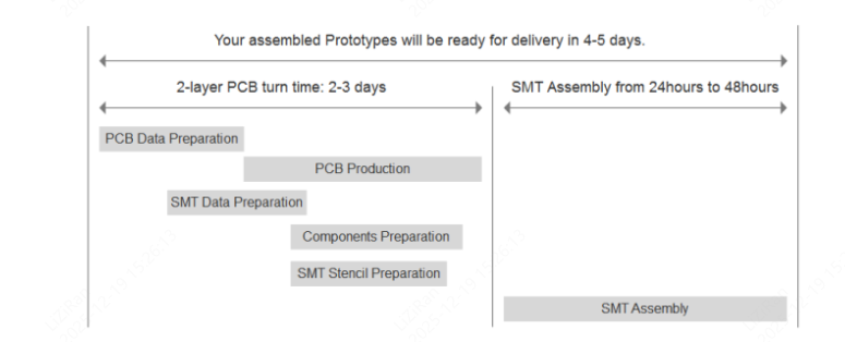
At JLCPCB, the standard SMT assembly workflow is carefully engineered to maximize efficiency. By adopting a parallel engineering approach, we intentionally overlap PCB fabrication time with SMT preparation activities, enabling industry-leading ultra-short delivery cycles.
1.1 Clear Definition of Standard Lead Times
To avoid ambiguity, we first define two key lead-time concepts:
- PCB Fabrication Lead Time (Build Time): The period from the actual start of physical manufacturing (shown as “MI Started” in the production status) to the completion of PCB fabrication, when boards are ready to be transferred to the shipping center.
- SMT Assembly Lead Time: The pure production time starting from the moment the bare PCBs arrive at the SMT production line, covering all processes including component placement, soldering, inspection, and final packaging for shipment.
1.2 Parallel Engineering: The Foundation of Rapid SMT Assembly
Our promise of “fast assembly immediately after PCB completion” is not achieved by compressing a single process step. Instead, it is enabled by a mature and well-established parallel engineering system.
The core principle is simple: All SMT preparation activities are initiated and completed in parallel while the PCB is still under fabrication.
This means that while your PCB is still on the manufacturing line, our systems are already processing the following tasks simultaneously:
- PCBA Engineering Data Processing: DFM analysis and assembly preparation are performed based on the pick-and-place files and silkscreen data to accurately define component placement locations.
- Stencil Fabrication: Based on internally generated stencil design data, high-quality, dedicated solder paste stencils are laser-cut in advance.
- Component Kitting and Verification: All required components are rapidly picked, verified, and prepared from JLCPCB’s extensive parts library.
Thanks to this parallel workflow, over 90% of PCB assembly orders complete the entire SMT process within 24–48 hours after PCB fabrication is finished. Once the PCB comes off the production line, it can be transferred directly to the SMT line with virtually zero waiting time, enabling true relay-style manufacturing.
1.3 Total Lead Time Illustration
Therefore, the total delivery time of your project can be clearly expressed by the following relationship:
2. Why Can the Actual Lead Time Vary?
Although we strive to deliver consistent and predictable lead times through parallel engineering, every order must pass through several critical preparatory stages before entering high-speed production.
These stages involve necessary interactions with you and are essential to ensuring final product quality. However, they may also affect the overall schedule. Understanding these steps will help us collaborate more efficiently.
2.1 Review and Confirmation Stage
This stage ensures that your design files can be manufactured accurately and reliably and serves as the official starting point of production.
- PCB Design Review: A preliminary manufacturability review is conducted on the submitted design files. To ensure smooth production, we recommend that your design complies with the manufacturing capabilities published on our official website. The final responsibility for design details and functional implementation remains with the customer.
- Advanced Options Confirmation: All selected advanced services and special remarks submitted during order placement are reviewed to confirm technical feasibility and process compatibility.
- Component Library Creation: If the BOM includes components without an existing footprint or placement library, our engineering team will create an accurate assembly library for those parts. This process requires additional time and is typically completed within 48 hours.
During the review phase, additional payment requests may be generated if required. To avoid delays, we recommend completing any pending payments promptly via the order history page.
2.2 Engineering Data Preparation
Once the review is approved, we generate detailed, order-specific engineering documentation. During this process, issues requiring customer confirmation may be identified, including but not limited to:
- ① Unclear Component Polarity or Orientation: Polarity markings on the PCB silkscreen are unclear or inconsistent with industry standards.
- ② Component Selection or Footprint Mismatch: The selected component does not match the corresponding pad or footprint design.
- ③ Component Placement Clearance Risks: Insufficient spacing between components may lead to solder bridging, short circuits after reflow, or difficulties during rework and repair.
2.3 Production Stage
Even after all engineering data is confirmed and the order enters production, customer confirmation may still be required under certain conditions:
1. In-Process Manufacturing Confirmation: If abnormalities or unexpected conditions are identified during production, we may need to consult with the customer before proceeding.
2. Execution of Advanced Options: If advanced services such as component baking are selected, the required process time (e.g., 48 hours) is already calculated and included in the total lead time displayed in the system. These services do not cause unplanned lead-time extensions.
Summary: How to Interpret a “Pending” Order Status
In general, if your order status remains “Pending” for an extended period, it indicates that the order is awaiting your confirmation on an engineering or production-related issue.
During this time, the production “clock” is paused and will resume only after we receive your explicit feedback.
Timely confirmation from the customer is the most effective way to keep the order moving forward.
3. How to Use Our Expedited Services
For time-critical projects, JLCPCB offers clearly defined expedited service options to minimize overall delivery time.
Please note that all expedited services must be selected at the time of order placement, and final availability is subject to the specific process complexity of your order and current production capacity.
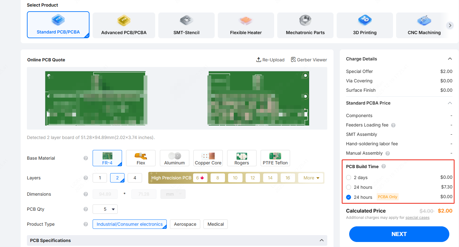
3.1 PCB Expedited Service
- How to Select: After uploading your Gerber files and completing the basic order parameters, you will find the “PCB Build Time” option on the PCB order page. You may choose from the available expedited tiers.
- A Key Advantage: For integrated PCBA orders (PCB + SMT assembly), we provide complimentary 24-hour PCB fabrication by default to accelerate the overall project timeline. Please review this option carefully during order placement.
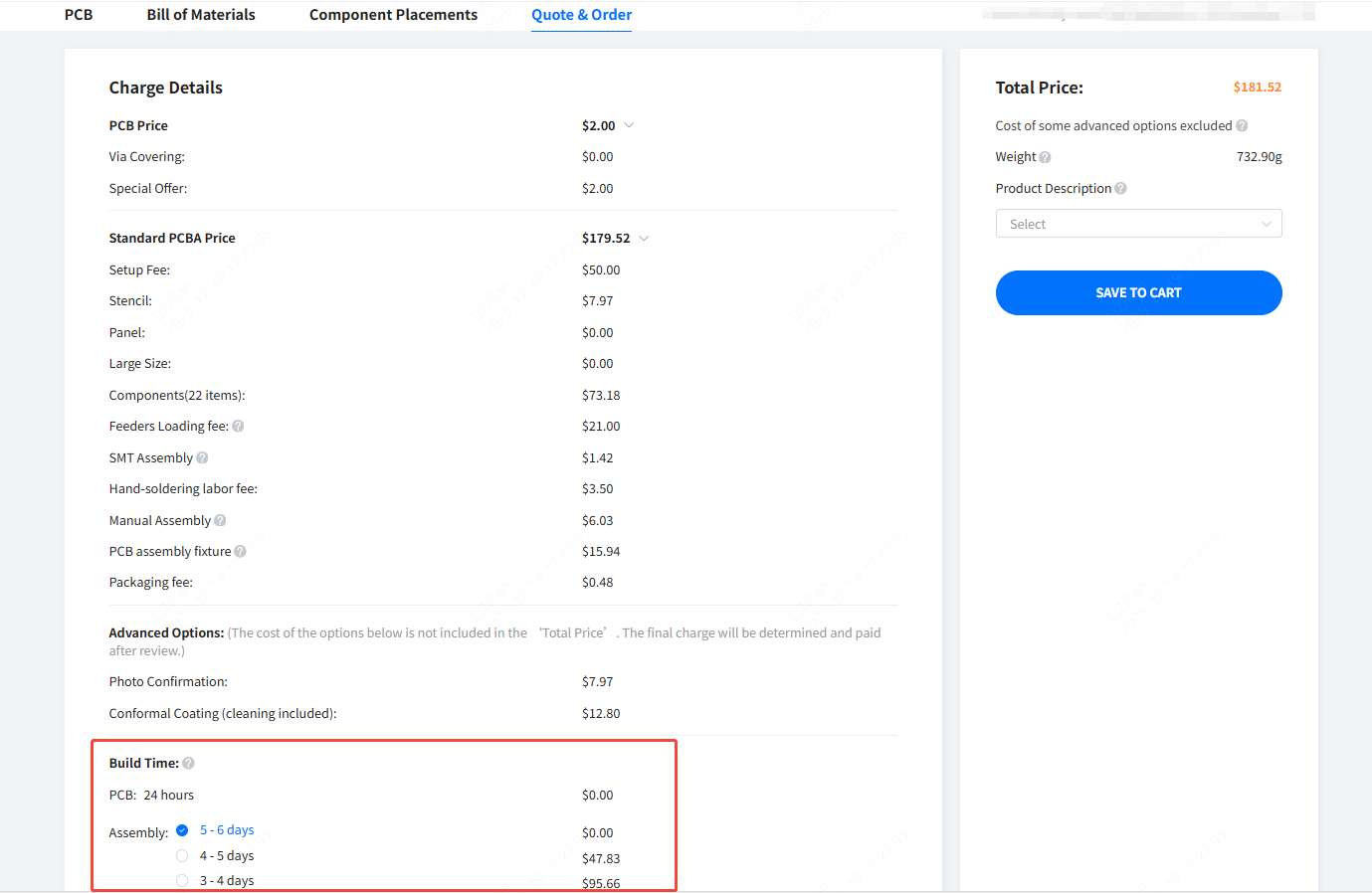
3.2 SMT Assembly Expedited Service
- How to Select: SMT expedited options are selected at a later stage in the workflow. After completing BOM upload and component matching, you will find the SMT assembly expedited option on the final “Quote & Order” confirmation page before proceeding to the cart.
- Pricing and Lead-Time Reduction: SMT expedited service is charged on a per-day basis, with a standard rate of USD 47.83 per day. For example, if the standard SMT lead time for your order is estimated at 5–6 days, selecting “1-day Expedited SMT” will shorten the target lead time to approximately 4–5 days.
4. How to Track Your Order Progress
Having clear visibility into every stage of your order is essential for efficient project management. JLCPCB provides a transparent and intuitive online tracking system.
4.1 Access Path and Page Overview
You can monitor your order status through the following two pages:
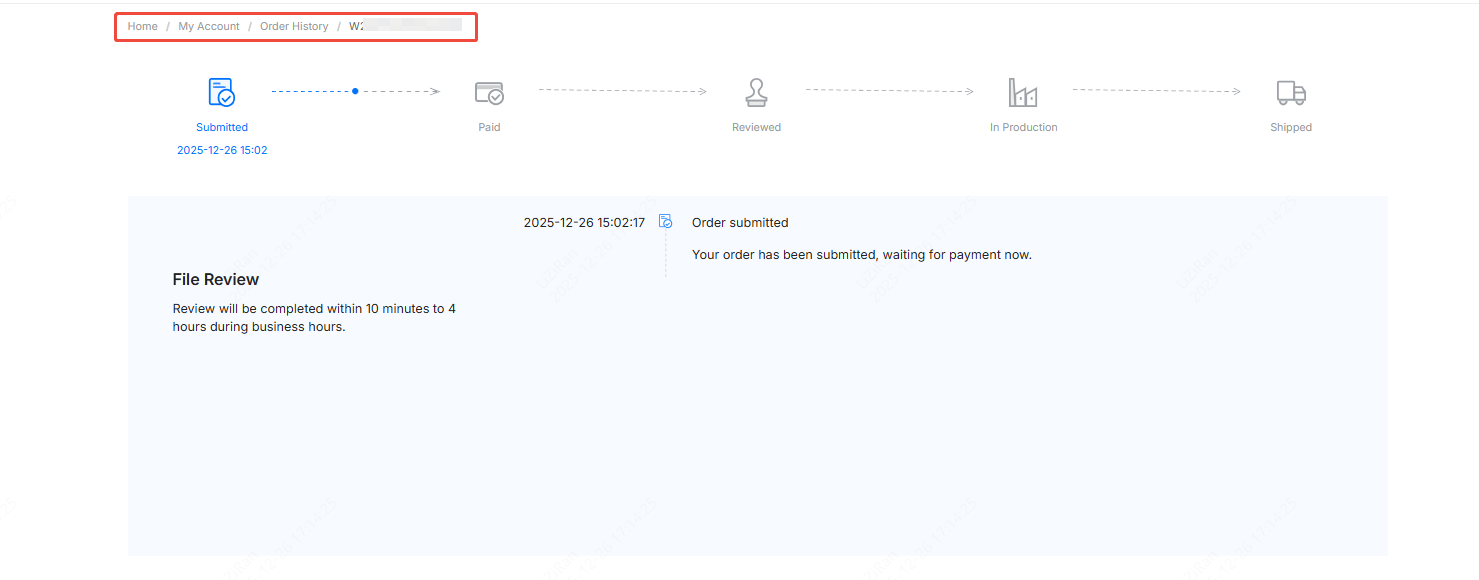
4.1 Overview of the Full Order Lifecycle
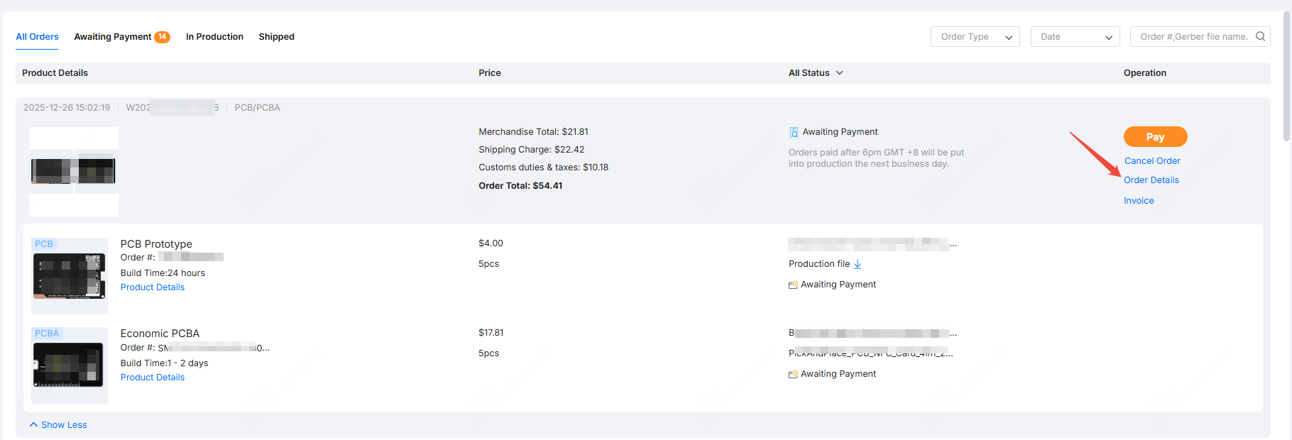
1. Navigate to Order History, then click Order Detail.
2. This page displays the complete order status flow: Submitted → Paid → Reviewed → In Production → Shipped, allowing you to quickly understand the overall progress at a glance.
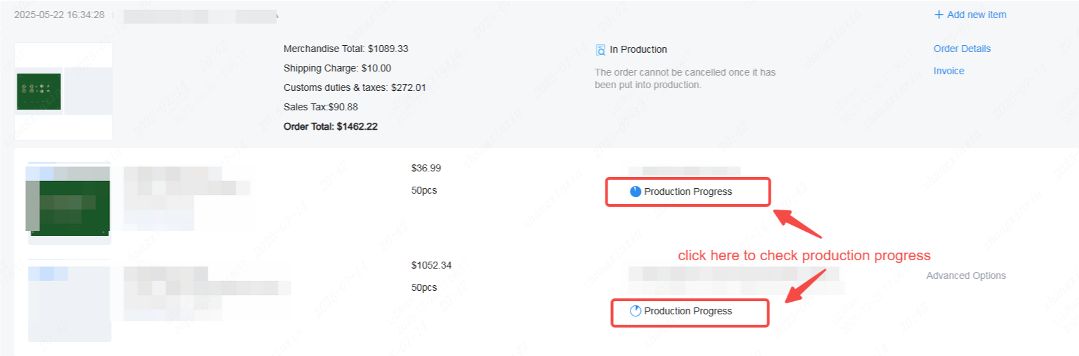
4.2 Real-Time Production Tracking
Within the Order Detail page, locate and click the Production Progress tab. This view shows detailed, real-time manufacturing milestones.
4.2 Key Recommendation
We strongly recommend using both views in combination:
- Use Order Detail to track major milestones.
- Use Production Progress to monitor specific manufacturing steps.
When the order status displays “Pending”, it usually indicates that your immediate confirmation is required. Timely customer feedback is the most critical factor in keeping production moving without interruption.
Best Practices for Smooth Order Execution
To ensure your order is completed as efficiently and smoothly as possible, we strongly recommend following the best practices below. These steps help prevent most delays and keep your project on schedule.
Before Placing an Order: Preparation Is Key
1. Design Self-Check: Before uploading your files, use our free online DFM tool to verify that your PCB design complies with manufacturing capabilities and process requirements, avoiding basic manufacturability issues.
2. Component Selection: Ensure that the selected components’ specifications and packages fully match your PCB pad and footprint design. Mismatched components (e.g., incorrect package types) are one of the primary causes of engineering confirmation delays and assembly failures.
After Placing an Order: Timely Response Ensures Continuity
1. Monitor Order Status and Communications: After placing an order, closely monitor both your order status and registered email inbox. When the status changes to “Pending”, customer action is usually required.
2. Respond Promptly to Engineering Inquiries: Please review and respond as soon as possible to DFM reports, component confirmations, or additional payment requests sent by our engineering team via email or internal messaging. Your timely feedback is the only way to release production holds and move the order forward.
3. Leverage Expedited Options When Needed: For urgent projects, make appropriate use of our PCB and SMT expedited services during order placement. Please note that expedited services are most effective only when accurate design files and fully kitted components are provided.
Final Note
A successful order is the result of a seamless collaboration between JLCPCB’s precision-driven parallel engineering system and your thorough preparation and timely responses.
By following the recommendations above, you can fully leverage JLCPCB’s high-efficiency manufacturing ecosystem and help ensure first-pass success and on-time delivery.