Introduction to JLCPCB Surface Finishes
Last updated on Sep 09, 2026

HASL - Hot Air Solder Leveling (Leaded)
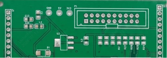
HASL (Hot Air Solder Leveling) is one of the most traditional and widely used surface-finish processes in the PCB industry. The PCB is immersed in molten solder (a tin-lead alloy), after which high-pressure hot-air knives remove the excess solder, leaving a tin-lead alloy coating on the copper pads. This coating protects the exposed copper from oxidation and, because the surface is already coated with solder, provides good wetting during subsequent assembly and soldering.
Thanks to its low cost and mature technology, HASL has long been the preferred surface finish for most general-purpose PCBs and DIY projects. However, the hot-air leveling process can produce variations in coating thickness across the pad surface. As a result, it is less suitable for fine-pitch components and packages such as BGAs that require a highly planar surface.
Process Characteristics:
• Typical coating thickness: approximately 1-40 micrometers
• Both the melting point of leaded solder and the HASL solder-pot temperature are relatively low
• The lead content of tin-lead solder can be as high as 37%, so it does not comply with RoHS environmental requirements
Advantages:
• Mature, low-cost process; one of the most economical surface finishes available
• Good oxidation resistance
Disadvantages:
• Insufficient surface planarity; unsuitable for fine-pitch components and BGA packages
• High-temperature thermal stress during processing may introduce PCB defects
• High lead content; does not meet RoHS environmental standards
• Extremely inconvenient for processing thin PCBs
Lead-Free HASL - Lead-Free Hot Air Solder Leveling
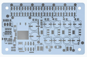
Lead-free HASL is the environmentally friendly upgrade to leaded HASL. It replaces conventional tin-lead solder with lead-free solder. The lead content is typically no more than 0.5%, meeting the requirements of the RoHS environmental directive.
Compared with leaded HASL, the main difference lies in processing temperature: the eutectic temperature of lead-free solder, the HASL solder-pot temperature, and the reflow temperature are generally all higher than those used for leaded HASL. These higher process temperatures place greater demands on the heat resistance of the PCB material and create more significant thermal stress. In addition, lead-free solder has slightly poorer wetting than leaded solder, and lead-free SAC solder joints have a comparatively dull appearance.
Process Characteristics:
• Complies with RoHS requirements
• Higher solder melting point and solder-pot temperature
• Coating thickness comparable to that of leaded HASL
Advantages:
• Environmentally friendly and lead-free; RoHS compliant
• Very mature process with a relatively low cost
• Excellent solderability
Disadvantages:
• Like leaded HASL, it does not provide sufficient surface planarity and is unsuitable for fine-pitch components
• Higher soldering temperatures impose stricter heat-resistance requirements on the PCB material and increase the risk of thermal stress
• Slightly poorer wetting than leaded HASL
• Likewise extremely inconvenient for processing thin PCBs
ENIG - Electroless Nickel/Immersion Gold
ENIG (Electroless Nickel/Immersion Gold) is one of the fastest-growing surface-finish processes in industrial applications. The process first deposits a layer of nickel onto the copper pads by chemical deposition, then deposits a thin layer of gold (approximately 0.025-0.05 micrometers thick) over the nickel through a displacement reaction. The nickel acts as a diffusion barrier that prevents copper and gold from diffusing into each other, while the chemically inert gold protects the nickel from oxidation during storage.
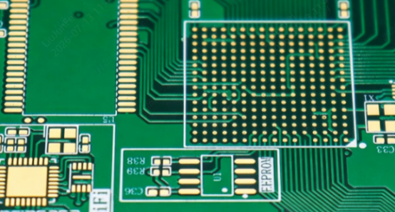
The key advantage of ENIG is its excellent surface planarity. Because it uses chemical deposition instead of hot-air leveling, ENIG produces a flat coating of uniform thickness on the pads, allowing components to sit flush against the pads for soldering. ENIG has become an excellent choice for complex components that require a highly planar surface. It is also RoHS compliant and suitable for thin PCBs (such as 0.4 mm boards) where HASL is restricted.
Process Characteristics:
• Nickel thickness: approximately 3-6 micrometers; JLCPCB offers gold thicknesses of 1 or 2 microinches
• Chemical deposition with no high-temperature processing, so the PCB material is not subjected to thermal stress
• Complies with RoHS requirements
• Excellent oxidation resistance
Advantages:
• Excellent surface planarity; suitable for BGAs, fine-pitch components, and other high-density packages
• Environmentally friendly and lead-free; RoHS compliant
• Excellent corrosion resistance
• Suitable for thin PCBs and other applications where HASL is restricted
Disadvantages:
• Higher cost and significantly affected by fluctuations in gold prices
• Risk of the "black pad" defect, which may affect solder-joint reliability
OSP - Organic Solderability Preservative
OSP is an environmentally friendly, lead-free surface-finish process. During OSP processing, a chemical reaction forms an extremely thin organic protective film on the copper foil, protecting the copper pads from oxidation during storage. During reflow soldering, the flux dissolves and removes the organic film, allowing the molten solder to bond directly with the fresh copper surface. Because the coating is extremely thin and uniform, it provides excellent surface planarity and can meet the soldering requirements of high-density circuitry, BGAs, and other complex components.
It can withstand four soldering operations, including two reflow cycles and two wave-soldering cycles. Unopened finished boards have a typical shelf life of up to three months under normal storage conditions.
Advantages:
• Excellent board-surface planarity: The surface is flat and smooth, making it suitable for high-density circuitry and BGA packages. Because HASL has inherent planarity limitations, JLCPCB has long excluded it from the options for 6-layer and more advanced PCBs, using high-planarity finishes such as OSP instead.
• Outstanding cost-effectiveness: OSP is available at no additional charge. By comparison, ENIG incurs a substantial surcharge per square meter because of fluctuations in gold prices. Choosing OSP can significantly reduce manufacturing costs.
• Mature and reliable process: Refined over decades, the process is supported by a robust quality system and meets the reliability requirements for serving JLCPCB's large customer base.
Disadvantages:
• Not suitable for gold-finger connectors: OSP cannot be used on wear-resistant, conductive contact surfaces such as mating gold fingers.
• Not suitable for castellated-hole module boards: If a long delay occurs before a second soldering operation, secondary solderability is significantly poorer than with ENIG.
| Process | Advantages | Disadvantages |
| HASL (Leaded) | Mature, low-cost process; good oxidation resistance | Insufficient planarity; unsuitable for fine-pitch components/BGAs; high lead content (up to 37%) and not RoHS compliant; inconvenient for thin-PCB processing |
| Lead-Free HASL | Environmentally friendly and lead-free; RoHS compliant; mature process with a relatively low cost; excellent solderability | Insufficient planarity; unsuitable for fine-pitch components/BGAs; higher soldering temperature and greater thermal-stress risk; inconvenient for thin-PCB processing |
| ENIG (Electroless Nickel/Immersion Gold) | Excellent surface planarity; suitable for BGAs, fine-pitch components, and other high-density packages; environmentally friendly and lead-free; RoHS compliant; excellent corrosion resistance; suitable for thin PCBs and other applications where HASL is restricted | Higher cost and affected by fluctuations in gold prices; potential risk of the "black pad" defect |
| OSP (Organic Solderability Preservative) | Excellent board-surface planarity; suitable for high-density circuitry and BGAs; outstanding cost-effectiveness with no additional charge; mature and reliable process | Not suitable for wear-resistant, conductive contact slots such as mating gold fingers; not suitable for castellated-hole module boards |