Instructions for JLCPCB PCB Layout Ordering
Last updated on Apr 02, 2026
PCB Type Definition
Normal board
1. All holes on board are through-hole type, excluding blind holes and buried holes.
2. The design has little high-frequency signals, high power supplies and so on.
3. The overall component placement is not dense and compact, relative to the board dimension.
Power Supply board
1.Power supply region is beyond 30% of the design.
2. No high-frequency signal or high-speed signal.
High speed or high-frequency board
1. The frequency of designated signals is not smaller than 1Ghz.
2. Wave length exceeds 1 meter and the working frequency exceeds 500Mhz.
3. Have demand for EMI and radiation control.
4. Board type: Rogers or PTFE.
HDI (High Density Interconnector)
1. Microvias whose inner diameter is below 6mil(0.15mm) and outer diameter is below 0.25mm. Pin density is greater than 130 pins/square inch. Routing density is greater than 170 inches/square inch. Line width/spacing is lower than 3mil/3mil.
2. With 8 or more than 8 layers and compact component placement.
PCB dimension
Normally, if there is no special requirement for board outline, we will build and use a rectangular outline by default.
If there is no requirement for PCB board outline, you can fill in a size limit. During the process of designing, we will try to keep the size under your limit. If the design doesn't meet the limit, we'll negotiate with you about the settlement.
PCB Layer Count
The number of layers is necessary even if it's not critical. Layer count could also be deemed as the maximum and among values available, we'll choose the most optimized scheme for layer count and stack-up structure.
If there is any special requirement for layer count and stack-up structure, we'll complete design according to requirement as much as possible. If the design doesn't meet the limit or requirement, we'll negotiate with you about the settlement.
Pad Count
Pad count is a sum of pads on board, including through-hole type and surface mounted type.
Upload Files
Layout Requirements
The file, uploaded finally in xlsx format, records demand in detail for smooth process of designing. We provide a template for customers to fill out in ordering page.
Schematic & PCB file
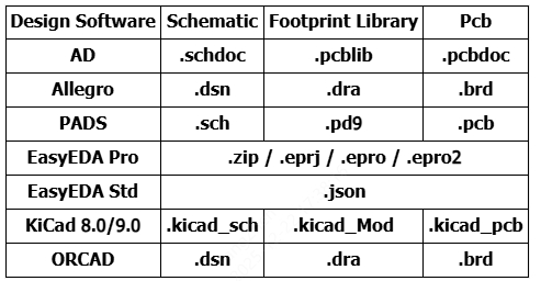
The file, uploaded finally in zip or rar format, should include the schematic and PCB files ouput by any EDA tool. (EasyedaPro is recommended.)
Please include all footprints in PCB file if possible.If your design does not include assigned footprints, we may charge an additional fee and request relevant documents (such as BOM lists and component datasheets) for footprint creation.

Other Files
The file, uploaded finally in zip or rar format, should include other related files like DXF file, datasheets which are helpful to specify special demand.
Deliverables
1. Gerber: 274X, for PCB Production
2. CPL(Component Placement List) File: xls, csv format for PCB Assembly
3. BOM (Bill of Materials) File: xls,csv format, for Component Procurement and PCB Assembly
4. DXF:CAD Structural Diagram for PCB Structure
5. 3D Model File:PCB enclosure, OBJ format by default(STEP format, exclusive to EasyedaPro)
6. Assembly Drawing:PDF format, Top and bottom silkscreen assembly drawing
7. Source/Design document
8. PCB Production Instructions:PCB Production Instructions, Processes, Impedance, Layer Stackup, etc.
Back to ordering page: https://design.jlcpcb.com/quote?spm=Jlcpcb.PCB_Layout