How to Prevent FPC Pad Lifting: 8 Design Solutions Tested
Last updated on Oct 19, 2026
Pads are the core medium for soldering components to a circuit board, and soldering quality directly determines the service life and reliability of the end product. Pad pull strength refers to the bonding force between the pad and the substrate.
FPCs use TPI or PET as the insulating layer. These materials are relatively soft and thin. Both TPI and PET are thermoplastic materials, meaning they soften when heated and harden when cooled. Taking ordinary TPI as an example, its maximum temperature resistance is 280 deg C. During manual soldering, the soldering iron temperature usually reaches above 320 deg C. The TPI material rapidly softens and shrinks. In addition, copper and TPI have different coefficients of thermal expansion, so their expansion and contraction differ, making pads prone to lifting.
This article uses different pad-design methods to avoid pad lifting and improve bonding force.
I. Experimental Design
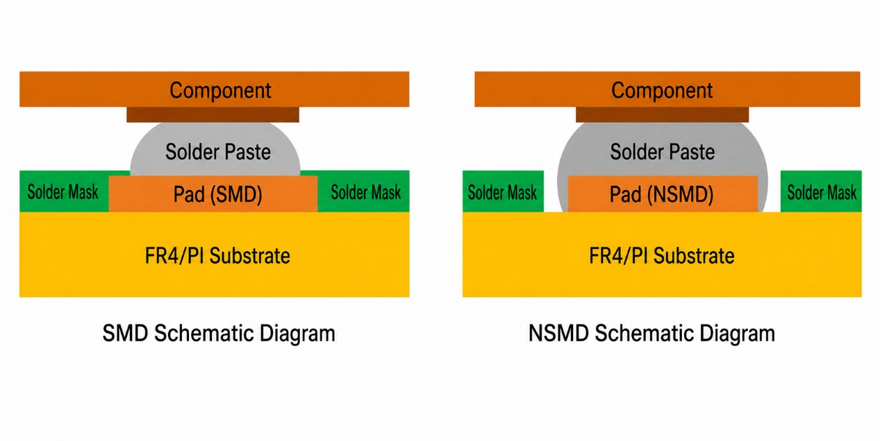
A total of 8 different pad solutions were designed. Each solution includes 6 modules, and each module has two groups of pads in different sizes: 0.7 x 1.5 mm and 1.1 x 1.8 mm. The goal is to study the effect of different modules and pad sizes on bonding force.
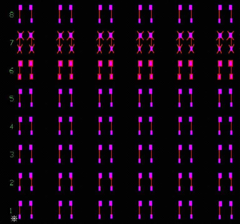
Solution Gerber data
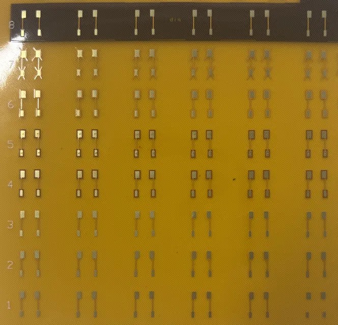
Physical board
Solution details
| No. | Solution description | Illustration |
|---|---|---|
| 1 | NSMD pad design (non-solder-mask-defined PAD design), with no pads or openings on the bottom layer | 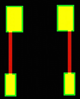 |
| 2 | NSMD pad design (non-solder-mask-defined PAD design) with teardrops added, with no pads or openings on the bottom layer | 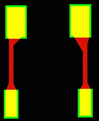 |
| 3 | NSMD pad design, with top and bottom pads and solder-mask openings of the same size | 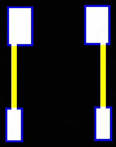 |
| 4 | NSMD pad design, with bottom-layer pads and solder mask 0.6 mm larger than the top layer |  |
| 5 | NSMD pad design, with bottom-layer pads and solder mask 0.6 mm larger than the top layer, and a 0.3 mm diameter hole added in the middle of the pad | 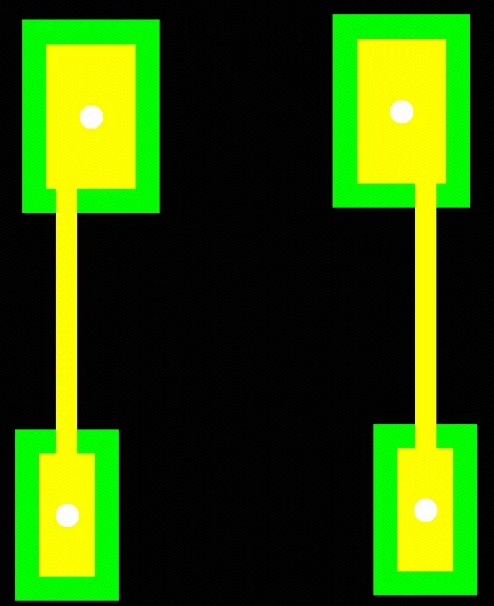 |
| 6 | SMD pad design (solder-mask-defined PAD design), with no pads or openings on the bottom layer |  |
| 7 | NSMD pad design with added lead-in traces, with no pads or openings on the bottom layer | 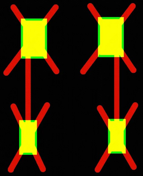 |
| 8 | NSMD pad design (non-solder-mask-defined PAD design) with added stiffener |  |
Solution details
II. Test Method
A wire was soldered to each pad. A pull-force tester was used to perform pull tests on each pad under the same parameters until the pad lifted, and the maximum pull-off force of each test was recorded.
Play
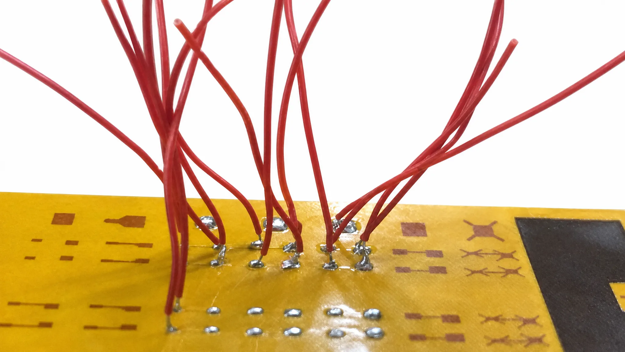
Soldered wire result
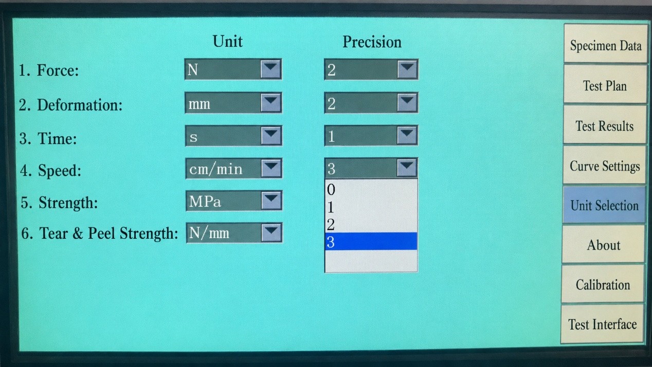
Test parameters
III. Test Results
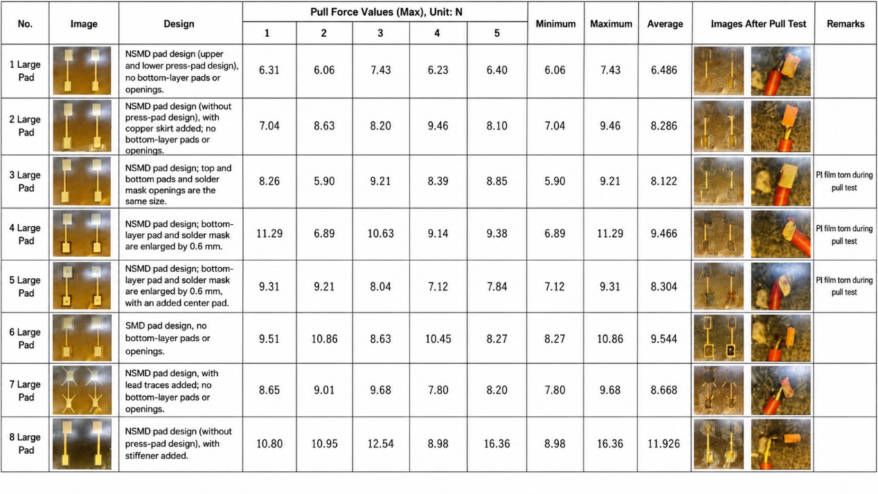
1. Pull-force data for 1.1 x 1.8 mm large pads:
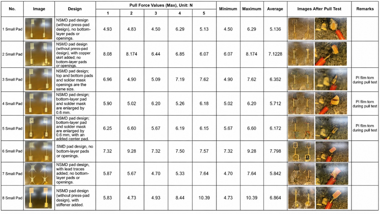
2. Pull-force data for 0.7 x 1.5 mm small pads:
IV. Experiment Summary
1. Designing the pad as an SMD solder-mask-defined PAD or adding a stiffener on the back significantly improves pad lifting.
2. When solder-mask-defined PAD design or a stiffener cannot be used, adding teardrops to the pad can also improve bonding force.
3. It is not recommended to design pads on both sides as overlapping, especially not with equal pad and opening sizes on both sides. In the experiment, these designs caused pad tearing.
4. FPC pads are not recommended to use an NSMD design, as this can easily cause pad lifting.
Need help optimizing your FPC layouts? For detailed parameters, please check our JLCPCB Capability Guide or explore more in the JLCPCB Help Center. You can also upload your Gerber files to get an instant quote and a complimentary DFM (Design for Manufacturing) review from our engineering team. 👉 Get an Instant Quote for Your Flex PCBs Today!