FPC Design Clearance Guide: Avoid Pad Lifting & Shorts
Last updated on Oct 19, 2026

Unlike rigid PCBs, FPC design demands strict control over safety clearances due to its flexible nature and complex fabrication process.
Seemingly minor trace or pad distances can easily trigger critical defects like pad lifting, trace cracking, or circuit shorts during lamination and assembly.
Today, let’s dive into the common clearance traps in FPC design to help you optimize your layout for flawless manufacturing.
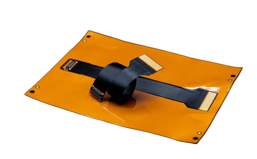
I. Solder Mask Design
1. Insufficient solder-mask bridge spacing
A solder-mask bridge is the solder mask between two pads. The distance between two pads must be at least 0.5 mm to retain the solder-mask bridge; otherwise, the bridge will be too thin and easy to break.
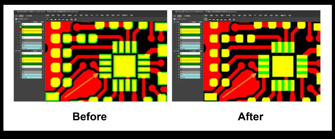
2. Distance from solder-mask opening to copper
The distance from a solder-mask opening to copper must be at least 0.15 mm. If this distance is too small, coverlay offset may expose copper in adjacent areas, creating a solder-bridge short risk when components are mounted.
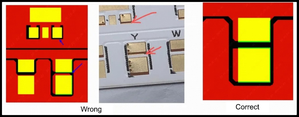
3. Solder-mask opening length
The solder-mask opening length should generally not exceed 20 mm, and large-area openings should be avoided. If the solder-mask opening is too large, it can be stretched and deformed during lamination, making bonding difficult or causing misalignment.
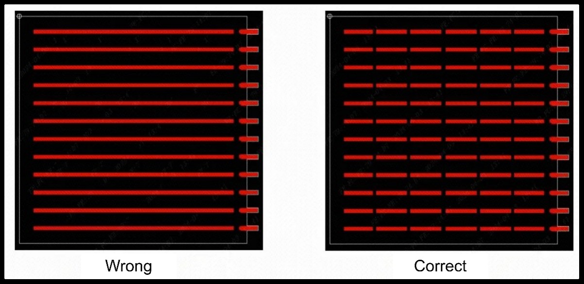
II. Outline Design
1. Distance between pads and the outline
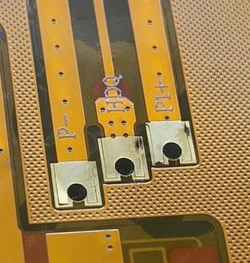
Pads must be more than 0.2 mm away from the outline; otherwise, laser cutting may cause carbonization and create shorts between pads.
III. Drilling Design
1. Distance between vias and board edge
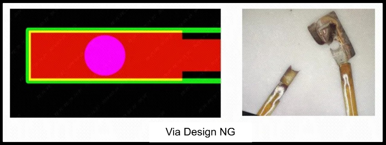
The distance from the via edge to the center of the board outline must be at least 0.5 mm; otherwise, the laser may damage the via and cause pad cracking. Vias should also not be arranged in a straight row; they should be staggered left-right or up-down.
2. Distance between vias and openings
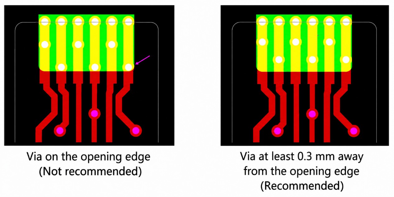
Vias must not be designed on the edge of an opening. They should be at least 0.3 mm away from the coverlay transition.
Because this area is a soldering finger area, it may bend during soldering. Stress concentrates at the transition between the coverlay-free and coverlay-covered areas, which may cause via copper cracking.
III. Circuit Design
1. BGA pad diameter
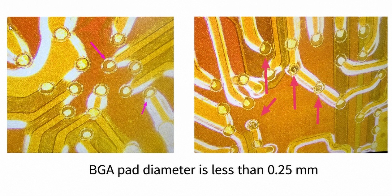
The BGA pad diameter must be at least 0.25 mm; otherwise, the finished pad may be too small or may lift.
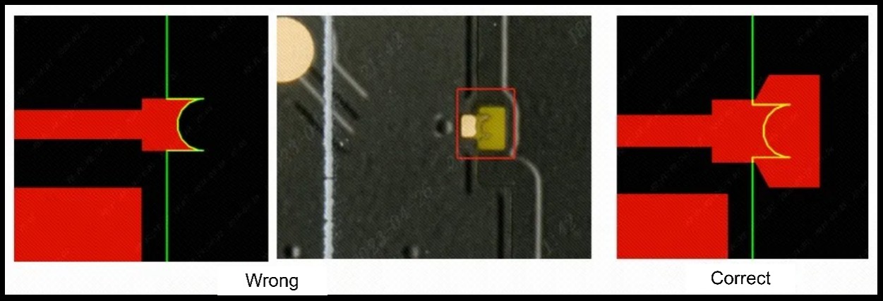
2. Board-edge pad width
Board-edge pads must be at least 0.5 mm wide, and the order notes must state that the pads must not be trimmed. Otherwise, JLCPCB will by default trim the pads 0.2 mm away from the board edge, which may cause pad lifting or cold solder joints.
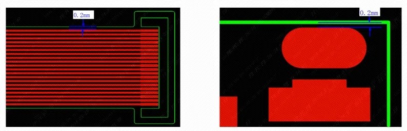
3. Distance from traces or copper pour to the board edge
To avoid copper damage during profiling, copper pours or routing must be at least 0.2 mm away from the outline. If the copper pour is flush with the board outline, when the CAM engineer pulls the board-edge copper 0.2 mm away from the outline, an open circuit may occur.
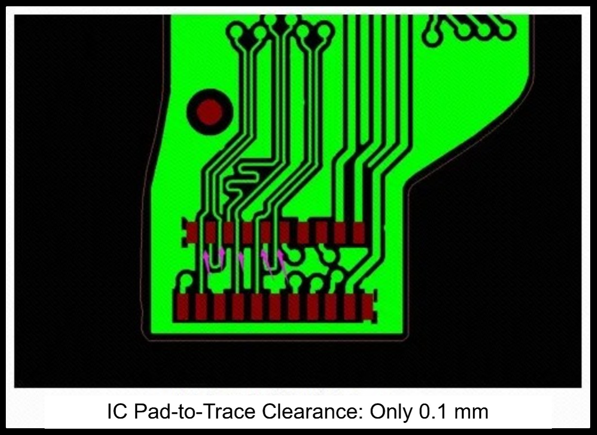
4. Distance from pad to trace
When the pad-to-pad spacing is less than 0.5 mm, avoid routing traces between pads whenever possible. The minimum pad-to-trace spacing should be 0.20 mm. It is recommended to route on the back side or accept exposed traces.
IV. Stiffener Design
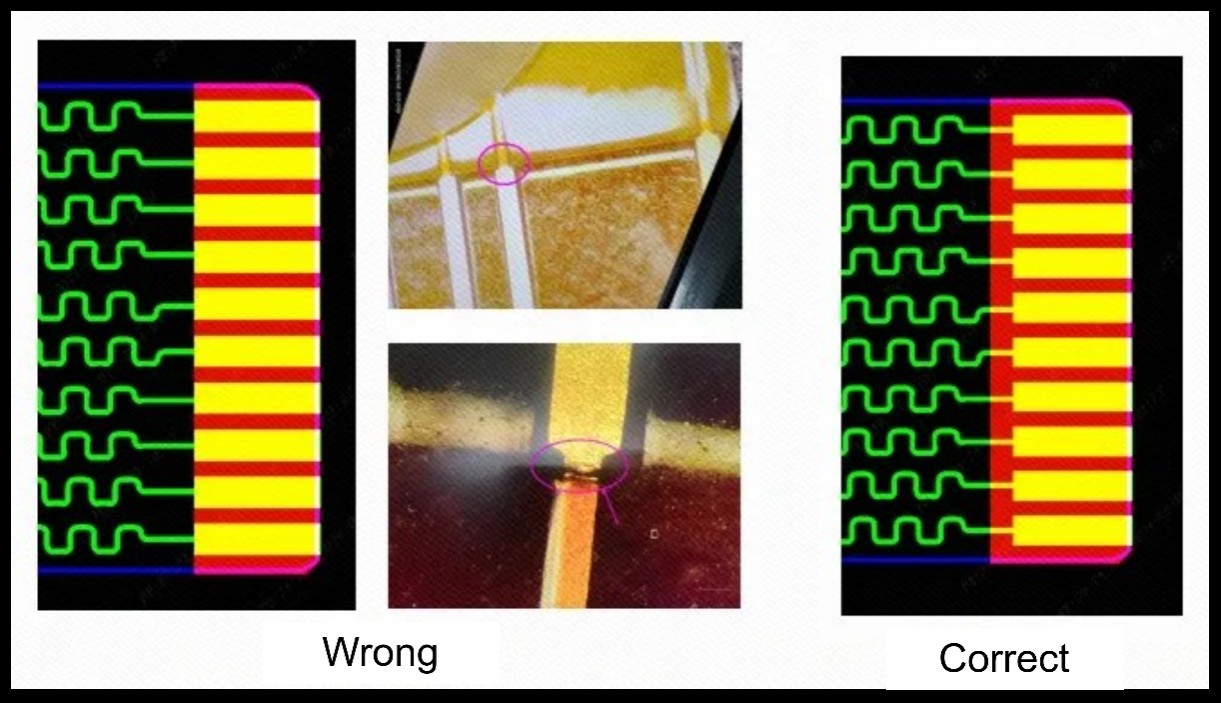
1. Distance between stiffener and pad
The stiffener area must extend at least 1.0 mm beyond the pad. If the spacing between the stiffener area and pad is insufficient, bending may crack the junction between the trace and pad, causing an open circuit.
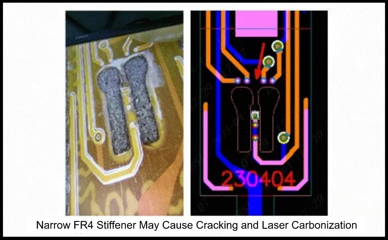
2. Minimum stiffener width
If the stiffener is too narrow, it is difficult to bond, easy to break, and prone to laser carbonization.
The following minimum widths must be met:
- Minimum FR4 width: 3 mm;
- Minimum PI width: 2 mm;
- Minimum Stainless Steel width: 1 mm.
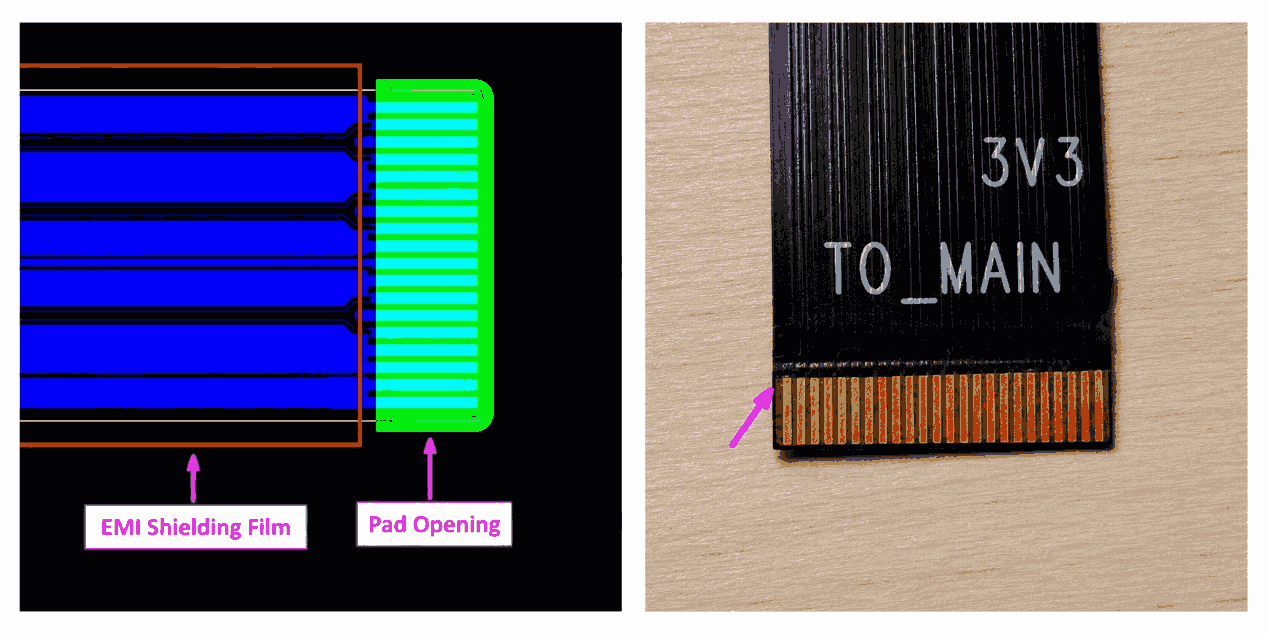
3. Distance from EMI Shielding Film to pad
Electromagnetic film is conductive. The distance from electromagnetic film to a pad opening must be at least 0.8 mm.
The data above comes from JLCPCB FPC production experience and is for reference only. It is intended to provide direction when setting design safety values and does not fully represent an industry standard.