Common PCBA After-Sales Issues & FAQs
Last updated on May 16, 2026
I. Appearance-Related Issues
1. Why is there flux residue on the PCB?
During the PCBA soldering process, we use high-quality, industry-standard no-clean flux. Any visible residue has the following characteristics:
- Non-corrosive: It does not cause corrosion or damage to circuits or components.
- High electrical insulation: It does not affect electrical performance, nor does it cause leakage or short circuits.
- Chemically stable: It remains stable under normal operating conditions and does not impact long-term product reliability.
What you may observe is a thin, transparent or light yellow, slightly tacky film, which is a normal and acceptable residue of no-clean flux. This condition is compliant with industry standards and is safe for use.
2. Why are there minor scratches on the PCB surface, even though the traces are intact?
1. During PCB fabrication and assembly, boards pass through multiple automated processes, including conveyor transfer, fixture contact, board flipping, and unloading. Minor surface friction between the PCB and manufacturing fixtures is unavoidable and may result in slight cosmetic scratches on the substrate. However, all PCBs undergo 100% electrical testing before shipment, ensuring that continuity, insulation resistance, and other critical electrical parameters fully meet specifications.
2. During packaging and transportation, external vibration or compression may cause slight movement of the boards inside the packaging, leading to minor surface abrasion.
3. To minimize cosmetic impact during shipping, we recommend selecting bubble-wrap packaging or separator packaging for future orders.
3. Why does the PCB show touch-up solder mask, resulting in slight color inconsistency?
During PCB manufacturing or component assembly, microscopic dust particles, air bubbles, or minor scratches may occasionally expose tiny copper areas in the solder mask layer. If left untreated, these exposed areas could potentially oxidize or affect insulation performance in humid environments.
Solder mask touch-up is a proactive and responsible corrective measure implemented to eliminate such risks.
This process may cause minor color variations on the PCB surface, but it does not affect electrical performance or long-term reliability.
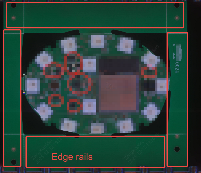
4. Why are there process rails (break-off edges) on the received boards?
For standard PCBA orders, we add 5 mm process rails on two sides of the PCB by default to ensure stable clamping and smooth transportation during SMT assembly.
- The minimum size requirement for standard PCBA orders is 70 × 70 mm.
- If the original PCB size is smaller than this, process rails are added to meet the assembly equipment requirements.
After receiving the boards, the process rails can be easily removed. Simply apply even pressure along the V-CUT scoring line to snap them off. No special tools are required. Once separated, you will obtain the PCB with its original design dimensions.
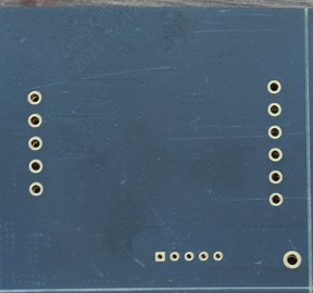
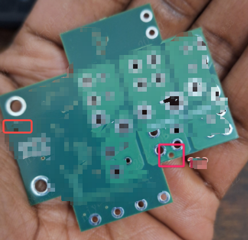
5. Why are there extra holes on the PCB? Why does JLCPCB add holes without authorization?
For economic PCBA orders, fiducial / tooling holes are essential for accurate component placement.
- Typically, two to three tooling holes are added, located near the PCB corners and spaced as far apart as possible to improve placement accuracy.
- The tooling holes are non-plated through holes (NPTH) with a diameter of 1.152 mm (45.4 mil) and a solder mask clearance of 0.148 mm.
These tooling holes are only applied to PCB assembly orders. We make every effort to place them in blank areas without routing or copper. If space constraints exist, they may be placed within copper areas, while ensuring no impact on circuit functionality.
II. Component Selection, Orientation, and Soldering Issues
1. Why are some components missing on the assembled boards?
Under normal circumstances, our production line assembles only the components explicitly selected by the customer at the time of order placement. Components that are not selected will not be procured or assembled onto the PCBs.
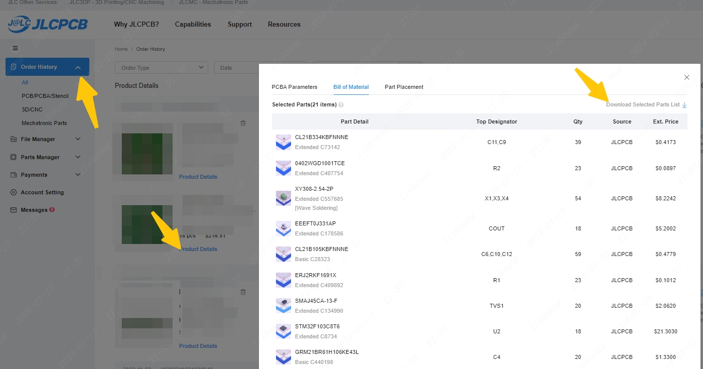
We recommend that customers carefully review the Selected Parts List in the order details and verify that all components listed in the BOM are included and selected before submitting the order.
2. Why do the assembled components differ from those listed in the BOM?
1. Please verify that the parameters specified in the BOM (such as part number, value, package, and electrical ratings) accurately correspond to the intended components.
2. In general, our system performs component matching based on the package type and description provided in the BOM. If a JLCPCB part number is specified in the BOM, the system will prioritize matching components with a “C-code”.
3. If you believe a system-level matching error has occurred, please provide clear close-up photos of the affected components as well as overall photos of the complete PCBA when submitting an after-sales request.
3. Why is the component orientation different from what the customer expected, even though it matches the DFM drawing?
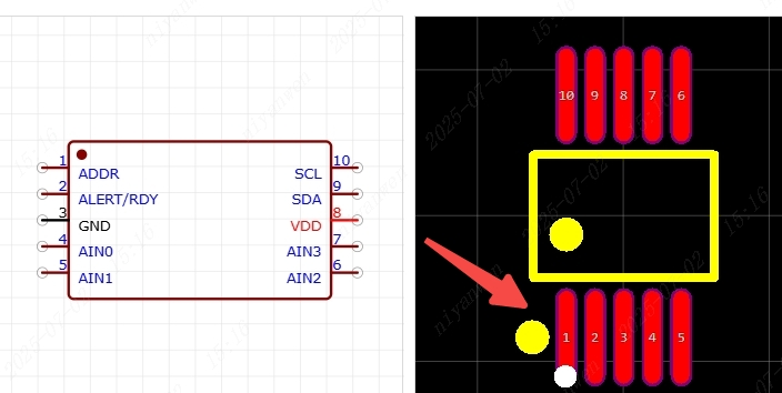
For every PCBA order, component placement is finalized prior to production based on the CPL (Component Placement List) file provided by the customer and the PCB silkscreen markings.
The silkscreen on the PCB clearly indicates component orientation, typically by marking Pin 1 with a dot or symbol. If you believe a component has been placed incorrectly, please verify that the production files (BOM, CPL, PCB) are consistent with the silkscreen orientation markings.
Common Silkscreen Orientation Conventions
1) IC / Chip Components
For SMT PCB designs, it is strongly recommended to place a silkscreen dot near Pin 1 of IC components.This standard marking method helps avoid engineering confirmation delays and potential misunderstandings during assembly.
Customers may refer to footprint libraries provided by the EasyEDA team for recommended practices.
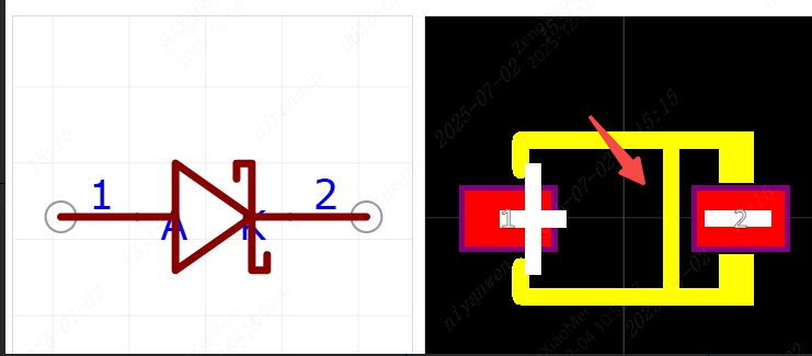
2) Diodes
Diodes are typically marked with a bar on one side, which represents the cathode (negative terminal).
Standard practice requires this bar marking to be clearly visible in both the component footprint and the PCB silkscreen layer.
Customers may refer to diode footprints provided by EasyEDA for reference.
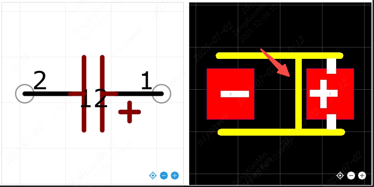
3) Tantalum Capacitors
Tantalum capacitors are typically marked with a bar indicating the anode (positive terminal).
This polarity marking should be consistently maintained in both the component footprint and the PCB silkscreen layer.
Customers may refer to the tantalum capacitor footprints provided by the EasyEDA team for proper orientation guidance.
III. After-Sales Compensation Policy
To clarify responsibilities and compensation criteria for potential component- or assembly-related issues in PCBA orders, the following policy applies:
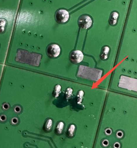
If finished products exhibit soldering defects (including but not limited to cold solder joints, solder bridging, insufficient solder, or missing solder joints), and such defects are verified to be attributable to our manufacturing process, compensation will be calculated based on the actual assembly (soldering) fees paid in the order.
The maximum compensation per board shall not exceed the unit price of the corresponding board.
Compensation Eligibility Conditions
Compensation applies only to defects caused during our manufacturing process, including:
- Open circuits
- Short circuits
- Intermittent via connections (partially open vias)
- Non-conductive vias
The following cases are excluded from compensation:
- Defects caused by incorrect or incomplete engineering data provided by the customer, including design-related open/short circuits
- Issues related to board outline, solder mask, silkscreen, tolerances, or other PCB design files
- Incorrect component selection, incorrect specifications, or mismatched part parameters provided by the customer
- Failures caused by improper operating conditions or external usage environments
Exclusions Related to Cosmetic Damage
Cosmetic damage, including but not limited to surface scratches or dents, that does not affect functionality or cause substantial impairment to product use, is not eligible for compensation.
Product Handling and Usage Exclusions
Compensation will also be void if the product:
- Cannot be tested due to misuse (including electrostatic discharge, ESD)
- Has been damaged due to negligence, accidents, or unauthorized modification
Customers are strongly advised to verify design files and BOMs before production thoroughly, and to perform necessary inspections and testing upon receipt to ensure the product meets expectations.
IV. Cases Not Covered by JLCPCB After-Sales Support
1. Customer-Supplied Components
JLCPCB assumes responsibility only for the soldering process of customer-supplied components.
If components exhibit performance degradation, incorrect parameters, or functional defects after assembly, such issues must be addressed directly with the original component supplier.
JLCPCB does not provide warranty or after-sales support for the intrinsic quality of customer-supplied components.
2. Pre-Ordered or Overseas Proxy-Purchased Components
For pre-ordered components or overseas proxy-purchased components, component selection and matching are performed by the customer.
JLCPCB acts solely as a procurement agent on behalf of the customer and does not assume responsibility for component selection errors.
- If the received components match the order specifications, but the customer later determines the wrong components were selected, such cases are not eligible for after-sales claims.
- If the received components do not match the order specifications, please provide clear photos of the components and overall photos of the assembled PCBA when submitting an after-sales request. We will verify and handle the case accordingly.
When using overseas procurement channels, customers are responsible for selecting qualified suppliers and confirming correct part numbers. JLCPCB does not assume liability for component selection errors in such cases.
3. Damage Caused During Testing or Use
If, during testing or use after delivery, components or PCBs are damaged due to non-quality-related causes (including but not limited to improper operation, incorrect wiring, abnormal power supply conditions, etc.), the resulting losses shall be borne by the customer.
Such cases are not eligible for after-sales complaints or quality compensation.
4. Design-Related Issues
Before submitting an after-sales claim, customers are requested to review the PCB design and component selection.
If PCB short circuits or functional failures are caused by customer design issues, such cases are not eligible for after-sales support.
Customers are generally advised to review the following items:
- ✔ Schematic design (particularly QFN pin connections)
- ✔ Component selection (verify against the BOM in order history)
- ✔ PCB fabrication files (accessible via order history)
- ✔ SMT DFM analysis reports (available in order history)
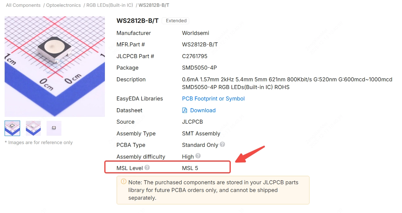
5. LED Assembly and Moisture Sensitivity Considerations
When assembling boards containing a large number of LED components, and where the Moisture Sensitivity Level (MSL) is ≥ MSL 3, we strongly recommend selecting the baking service before assembly.
Most LEDs are moisture-sensitive devices (MSDs). Failure to perform proper baking before assembly may negatively affect performance and long-term reliability.
In addition, we strongly recommend conducting a comprehensive functional test before shipment to ensure that all LEDs power on and emit light correctly. This step helps identify potential issues early and prevents failures during subsequent use.
If issues arise due to the omission of LED baking or shipment without adequate testing, such cases are not eligible for after-sales complaints or compensation.