JLCPCB PCB Layout FAQs
Last updated on Jun 10, 2026
What does JLCPCB Layout Service include and offer?
Basically, JLCPCB Layout Service includes components placement and routing and complete the design according to the schematic files provided by customers.
We do not provide schematic design or modification services, nor do we offer schematic-related suggestions. Any changes to the schematic must be completed by the customer, as these may lead to results that do not match your design intent.
What is the price of JLCPCB's PCB Layout services?
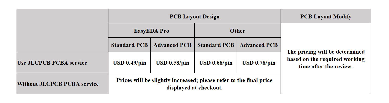
*Advanced PCB refers to HDI boards (design-only)and power boards.
*The minimum starting price for Layout services is as follows:
- PCB Layout Design: $100
- PCB Layout Modify: $120
*The final amount will be determined and displayed after the order has been reviewed.
*The pricing rules above are subject to adjustments. The final quoted price shall prevail after your order is reviewed and confirmed.
How long does it take to finish the PCB layout?
The estimated lead time is displayed in the form below. Delays may occur due to changes in design requirements or extensive communication needs.
Normally, customers could get an estimated lead time as the form shows above.
However, this is only for reference. Lead time may be modified by practice.
Lead time shall be referred to the quotation scheme. If an unexpected action during designing is caused by buyer's adjustment of design requirements, supplementation of materials or other matters that need to be communicated, the delivery time shall be postponed correspondingly.
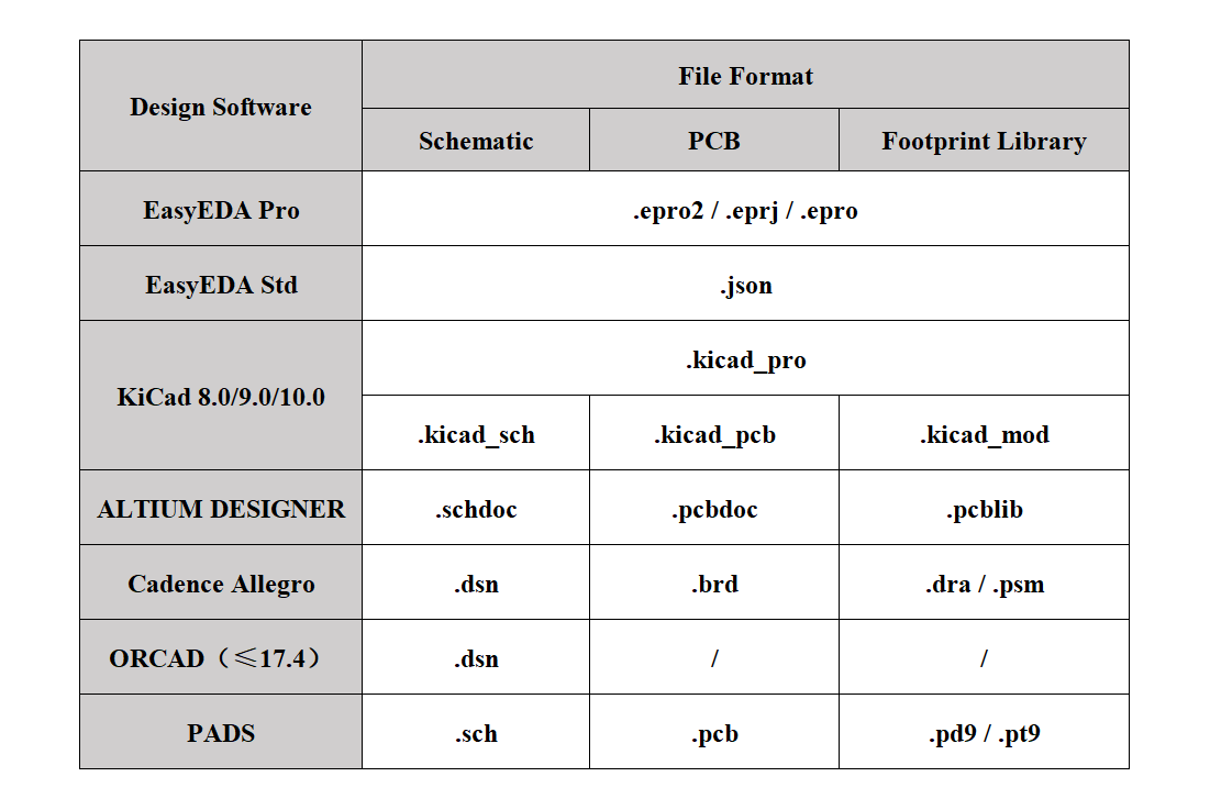
What software does JLCPCB Layout service support?
JLCPCB Layout service primarily uses EasyEDA. By designing with EasyEDA, you can benefit from faster delivery times and more competitive pricing. If you prefer other software, please indicate them when placing your order.
What documents are required for a PCB layout quote?
- Schematic file (parts with footprints required)
- PCB Layout design requirement illustrations
- Bill of Materials in Excel format (Optional)
- Component Datasheets / Component Footprint documents (Optional)
- DXF mechanical drawings (Optional)
- We may require you to provide the above optional documents in the following cases:
- If footprints are not included in your design: you must provide Item 3/Item 4 (additional fees may apply and will be confirmed before payment).
- For special structural requirements: you must provide Item 5.
What deliverables could we offer?
1. Gerber: 274X, for PCB Production
2. CPL(Component Placement List) File: xls, csv format for PCB Assembly
3. BOM (Bill of Materials) File: xls format, for Component Procurement and PCB Assembly
4. DXF:CAD Structural Diagram for PCB Structure
5. 3D Model File:PCB enclosure, OBJ format by default(STEP format, exclusive to EasyedaPro)
6. Assembly Drawing:PDF format, Top and bottom silkscreen assembly drawing
7. Source/Design document
8. PCB Production Instructions:PCB Production Instructions, Processes, Impedance, Layer Stackup, etc.
Feedback Reviews & Changes
Once the project has started, we will proceed with the layout according to the customer's requirements. We will notify you by email once the component placement is completed. You can view the placement on the order history page. It is the customer’s responsibility to ensure that the component placements and its footprints are satisfactory. Our team will make adjustments based on your feedback. After you confirm that the placement is satisfactory, we will continue with the routing. Upon completion of the routing, we will also notify you by email, and you can view the routing files on the order history page. Once you confirm the routing, we will deliver all necessary files to you.
Does the quote include fabrication fee? After using Layout service, will the project go into production automatically?
Our Layout services and fabrication services are separate departments and the systems have yet been integrated. Therefore, for now, customers need to place orders seperately.
Reverse Engineering&PCB Cloning/Copy/Duplication
JLCPCB Layout service does not support Reverse Engineering and PCB Cloning/Copy/Duplication now.
JLC's engineers will only make designs according to the schematic files provided by customers.
If customers only provide Gerber files or photos of the final product, JLC cannot offer help.
PCB Simulation
JLCPCB Layout service does not support it now.