Solder beading treatment for PCB stencil
Last updated on Jun 09, 2025
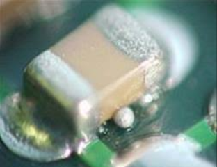
Solder beading, a defect that can result in short circuits, generally is related to an excessive solder paste deposit that, because of its lack of "body," is squeezed underneath a discrete component and then becomes a solder bead. The most common place to see solder beads are at the side of a chip components like resistors and capacitors.
Solder beading can be reduced substantially by decreasing the solder paste volume deposited on a printed circuit board (PCB).
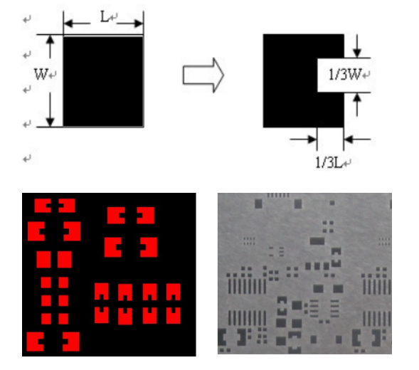
At JLCPCB, the stencil aperture for components(except for diode) larger than 0805 will be slightly reduced from the pad size like below image to avoid the solder beads.
Note: If you don't want to apply this solder beading treatment for your stencil, please make a remark when you place an order.