
Service Process
PCB layout is the process of converting the abstract connections of a schematic into a reality of a manufacturable Printed Circuit Board. Because of a good layout, a device's reliability, electromagnetic compatibility (EMC), and thermal stability will be defined. This guide will cover why PCB layout is important in modern PCB design, common technical issues that can undo a project, and why professional PCB layout services should be considered a strategic imperative in complex hardware.
Common Problems In Layout
Defects in Signal Integrity
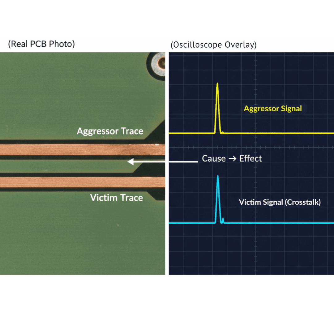
Defects in Signal Integrity In higher-speed circuits, traces act as transmission lines. A lack of attention to detail can cause the crosstalk between adjacent traces can affect signal integrity, impedance mismatches can produce reflections in the line, and timing errors can even spoil the data
Power Integrity Failures
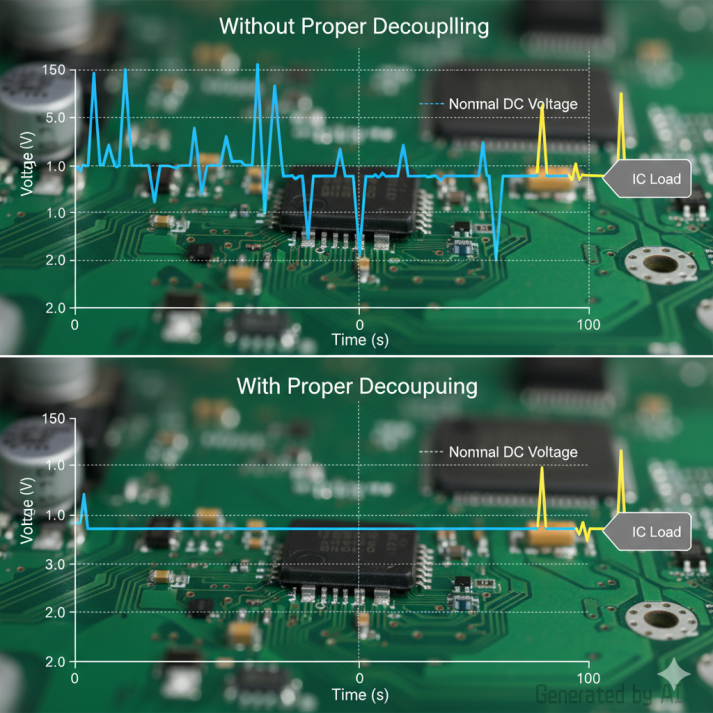
Power Integrity Failures An unstable power delivery network (PDN) is one of the more frequent intermittent, hard-to-debug problems. Common problems in this area involve excess voltage drop (IR drop) through high-current pathways or not enough Decoupling Capacitors to limit the voltage ripple on power rails to sensitive ICs
Thermal Management Problems
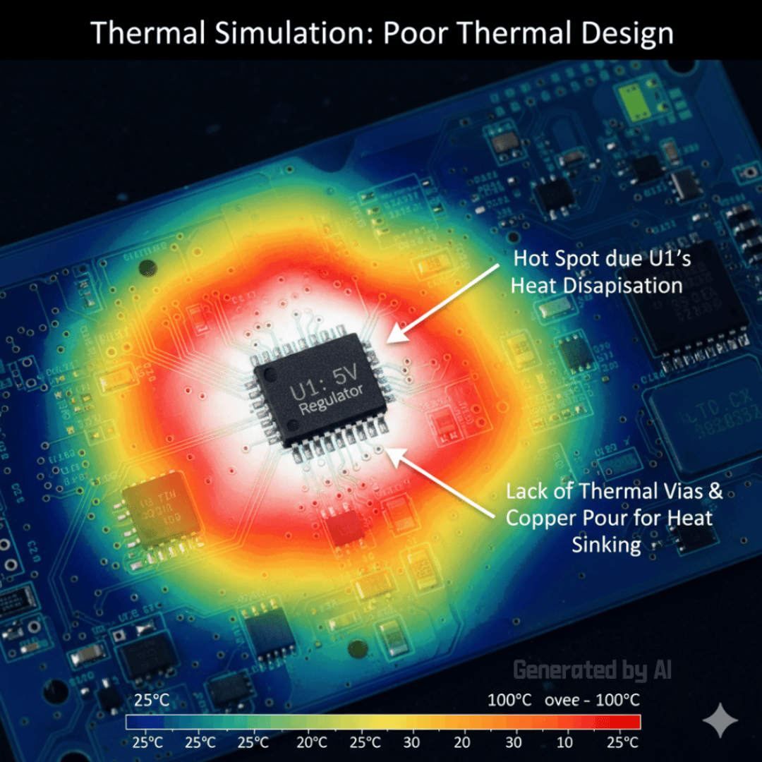
Thermal Management Problems Poor Thermal Design contributes to early-stage failure for components. High-power components that are placed too close to each other can create “hot spots” if there is an inadequate thermal path available to remove the heat. The end result is compromised performance and a greatly reduced assembly life.
Inattentive to Design for Manufacturability (DFM)
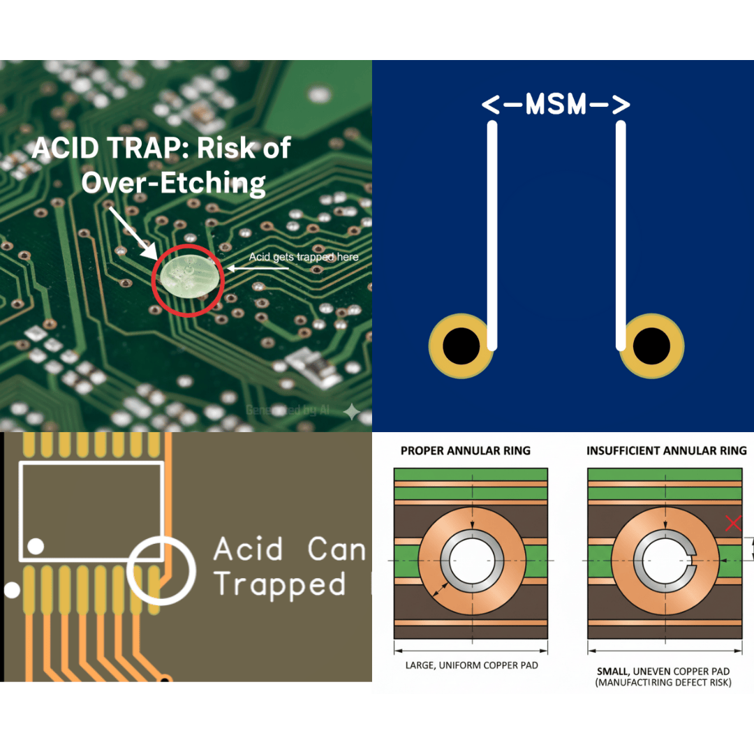
Inattentive to Design for Manufacturability (DFM) Inattentive to Design for Manufacturability (DFM): A design may perform perfectly in the lab, but cannot be manufactured reliably. DFM codes consist of conditions like creating acid traps (acute angles that entrap etching chemicals) or placing vias too near the pad, leading to substantially reduced manufacturing yields.
Acid Traps: Acid Traps: These are acute angles between traces that can "trap" etching chemicals during fabrication. This prevents the acid from being washed away properly, causing it to over-etch the copper and potentially create an open circuit
Insufficient Annular Ring: Insufficient Annular Ring: The annular ring is the ring of copper around a plated through-hole. If it's too small, minor drill wander during manufacturing can cause the via to break out from its connecting trace, resulting in a faulty connection.
Solder Mask Slivers: Solder Mask Slivers: These are tiny, thin slivers of solder mask that can occur between closely spaced pads. During processing, these slivers can detach, float around in the solder bath, and redeposit elsewhere on the board, potentially causing shorts.
FAQs
- Q: What files do I need to provide for a PCB layout service?
You will need to provide your complete schematic (preferably with footprints), a Bill of Materials (BOM), and any specific mechanical constraints or design requirements you have.
- Q:What is the difference between a schematic and a PCB layout?
A: A schematic is a logical diagram that shows how components are electrically connected. A PCB layout is the physical implementation of that schematic, defining the component locations, trace routes, and physical dimensions of the board.
- Q: How long does a professional PCB layout take?
The time required depends on the complexity of the board. A simple 2-layer board might take a few days, while a complex multi-layer, high-speed board could take several weeks. JLCPCB provides a timeline estimate in the quote.
- Q: Does this service include PCB simulation?
A: No, PCB simulation is not supported within the scope of the layout service at this time. The focus is on physical layout, routing, and DFM.
Convert The Schematic To PCB Easier!
Different PCB Boards In Layout: From Simple To Complex
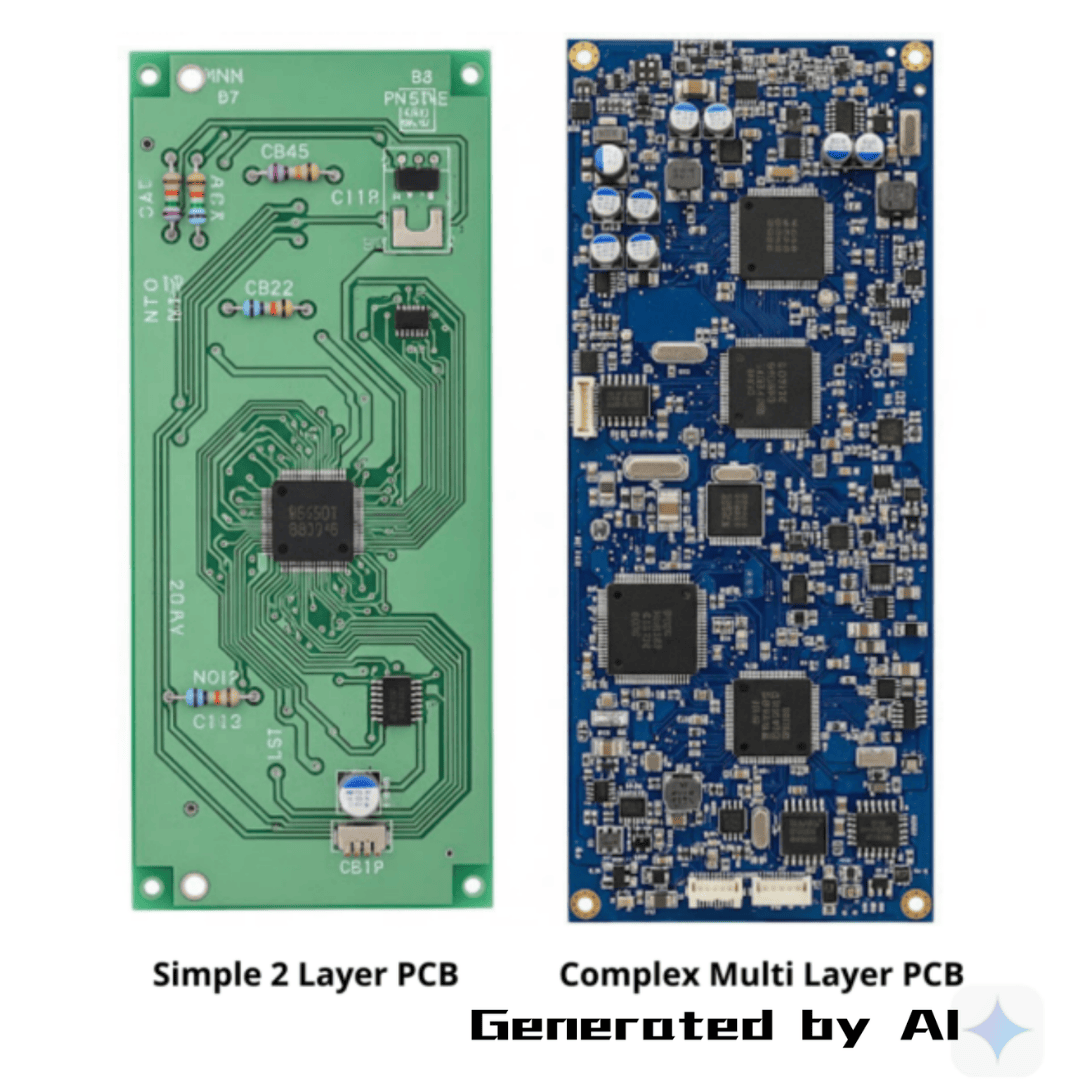
●Common Boards (2-4 Layers): Many embedded systems and IoT-based devices use these types of boards. They will often have low-speed signals, simpler power distribution, and our layout rules are more forgiving.
●Complex Boards (6+ Layers, HDI, RF): As we migrate into high-performance computing and wireless communications, the layout challenges increase multiplicatively.
●High-Density Interconnect (HDI): These boards have microvias and finer traces for higher density and require comprehensive planning.
●High-Speed Digital Boards: Designs that have interfaces like DDR memory use precisely controlled impedance and lengths of traces to match, in order to honor timing and signal integrity as specified.
Application Areas of Complex PCBs
Complex layout work is essential in today's most innovative technology sectors
●Telecommunications: For 5G base station and router RF PCBs, their layout requires complex RF PCB layouts having controlled impedance.
●High-Performance Computing: In motherboards and server backplanes, the density of routing is so extreme that it requires higher-layer count boards to reasonably manage it.
●Medical Devices: Portable diagnostic tools and wearable health monitors have such small design factors that achieving the density of routing requires HDI layouts.
The JLCPCB Layout Service Advantage
This is where a service like the JLCPCB PCB Layout Service provides immense value, acting as a strategic partner to overcome these challenges. It's a comprehensive service that converts your schematic into a manufacturable, high-performance PCB design.
● Manufacturing Integrated: This is the biggest benefit. The JLCPCB layout engineers have intimate knowledge of their own fabrication and assembly capabilities. They are designing with JLCPCB's specific DFM constraints from the get-go. Having manufacturing integrated into the layout eliminates the chance of a design getting rejected or having a low yield, which is common when design and fabrication are separated.
● Professional & Experienced Layout Team: Our team is comprised of professional engineers who can solve complex layout problems. We know how to lay out high-density boards, high-frequency circuits, and complex thermal management issues while maintaining a functional and reliable end result in the design. You are essentially gaining expertise that is hard to acquire in-house.
● Faster Turnaround Time: By working with a single process, the time-consuming back-and-forth communication that we usually go through with separately-designated design/drafting house and fabrication house is eliminated. They get it right on their manufacturing line the first time, shortening the lead time and getting your product launched sooner.
● Cost Savings: Being a PCB manufacturer means having significant experience in optimizing the layout board for cost-effective production. They can recommend the most effective layer stackup, via technology, and panelization strategy for your particular design, so you can save costs in production without compromising performance.
How JLCPCB Handles Your Order: A Streamlined Workflow
The process is made simple and collaborative and guarantees the layout meets your specific engineering requirements. It's a straightforward closed-loop experience:
1. Submit Your Requirements: You'll submit your schematic, your Bill of Materials (BOM), and any design restrictions that must be followed.
2. Engineering Review & Quote: Their engineering team will review your project and present you with a transparent quote.
3. Collaborative Layout Process: You'll have the opportunity to work with our professional layout engineers to finalize your design.
4. Review & Approval: You'll receive the completed layout files for review and approval.
5. Seamless Transition to Production: Once you approve of the design and the layout files are complete, we will send the files directly into JLCPCB's fabrication and assembly lines for production.
What to Expect: Professional Process and Deliverables
When you work with a professional layout service from JLCPCB, you're not simply receiving a completed design; you're receiving a full engineering package that is meant for successful production.
● The Workflow: The workflow is set up for maximum efficiency. It begins with a Quotation and Kickoff in which the team reviews your submission to validate the plan. The plan continues into the Layout Phase (stackup design, component placement) and Routing Phase (trace routing, DRC checks). The workflow ends with Finalization, in which you get the complete data package to consult and confirm.
● The Deliverables: THE JLCPCB service provides a complete set of handoff files. Working with JLCPCB, you receive Gerber 274X for fabrication, CPL for assembly, the BOM for sourcing, DXF for mechanical reviews, a 3D model file, and overall production documentation, including stackup and impedance information. Overall, the completed set of data means it is easy to hand off to any manufacturing facility.
● Software and Footprint Support: The service supports mainstream files from tools like Altium, Allegro, and KiCad. If your schematic is missing component footprints, the team can create them for you from datasheets, ensuring your library is complete and accurate.
When you engage with a professional layout service, you're not just getting a completed design; you're getting a comprehensive engineering package designed for successful manufacturing.
JLCPCB Layout
JLCPCB Layout services address issues such as signal interference dissipation, and Design for Manufacturability (DFM) in high - density layouts. We specialize in the pcb layout job of high - density boards for high - speed, high -frequency,and high - power applications, ensuring that your designs exhibit top - notch performance.
$80
Layout Coupon
Valid for 90 days