
How to Generate Gerber and Drill Files in Autodesk Eagle
Last updated on Apr 24, 2025
When you finished your design in Eagle, the last step before sending it off to the fab house is to generate the Gerber and Drill files. PCB fab houses will use these Gerber and Drill files to make your boards. Autodesk EAGLE includes a handy CAM (Computer-Aided Manufacturing) processor that allows you to load a CAM file and quickly generate the specific files you need for your design.
JLCPCB uses the Gerber format of RS-274X, Gerber X2 is not supported.
Install the CAM Files
First thing first, you need to download the predefined CAM files and store them in your computers.
Tip:The CAM files can be stored anywhere, but make sure it’s easy for you to find them. For example, if you store these files in Dropbox, this way you can use the same CAM files between different computers
Table 1. CAM Job Files for Different Eagle Versions
| Eagle Version | CAM Files |
|---|---|
| 8.6.0 to 9.6.2 [From 8.6.0, Eagle starts to use JSON format for CAM job files, the old CAM files are marked as "legacy".] | jlcpcb_2_layer_v9.cam |
| jlcpcb_4_layer_v9.cam | |
| jlcpcb_6_layer_v9.cam | |
| 7.2 to 8.5.2 [Start from Eagle 7.2 the old EXCELLON device output 2.5 format instead of 2.4 for drills, this caused the "Drill holes scale up 10x" issue in some Gerber viewers.] | jlcpcb_2_layer_v72.cam |
| jlcpcb_4_layer_v72.cam | |
| jlcpcb_6_layer_v72.cam | |
| 5, 6, 7.1 and Lower | jlcpcb_2_layer_v6.cam |
| jlcpcb_4_layer_v6.cam | |
| jlcpcb_6_layer_v6.cam |
Windows
Copy the CAM files to Users\your_user_name\Documents\EAGLE\cam folder.
GNU/Linux
Copy the CAM files to /home/your_user_name/EAGLE/cam folder.
macOS
To be done.
Generating the Files
1. Fire Up the CAM Processor
Just click the CAM Processor button.
[Users may also noticed there’s a "Generate CAM data" button next to the CAM Processor button, with one-click it can generate the CAM file based on the predefined template_2_layer.cam, but the generated files are note preferred by JLCPCB (The file extensions, lacks of flexibilities, etc.)]
Tip :For older Eagle versions, the CAM Processor icon may look different and the CAM Processor can be invoked from the File menu.
Figure 1. The CAM Processor button in Eagle 9.6.2
2. Load a CAM Job File
Now, you need to load the CAM job installed before, as shown below.

Figure 2. Load the CAM Job in Eagle 9
For old versions, the interface for loading a CAM job is different.

Figure 3. Load CAM Job in Eagle 7.1.0
3. Check Around
This CAM Processor has a built-in Gerber viewer which is pretty convenient, you can click on the layer items on the left and the Layer windows and the preview will be updated on the fly.
Check around, zoom in and out, this allows you to do a brief inspection on the Gerber file which will be exported.
In some cases, you may need to adjust the settings, please refer to Special Explanations section for details.
4. Process Job
If everything is OK. Click the "Process Job" button on the bottom right of the window. Now the magic happens! The CAM Processor will put all output files into a single ZIP archive, as shown below.

Figure 4. Job Processed Successfully
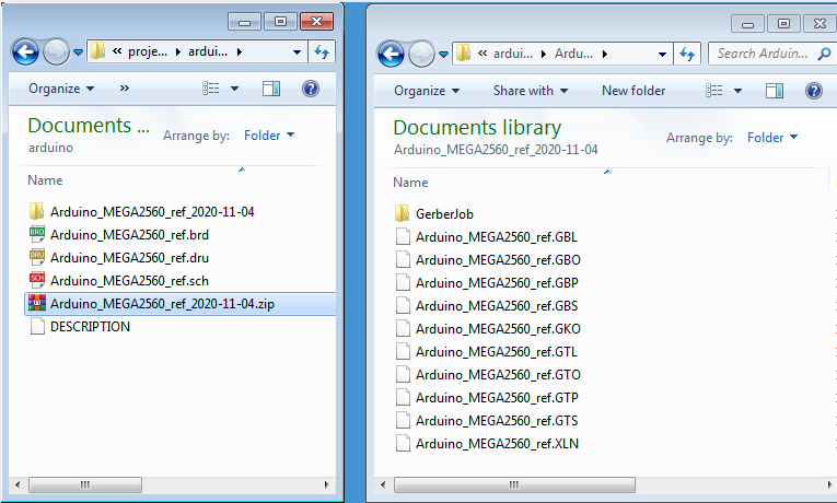
Figure 5. The Generated ZIP and the Files inside
For old Eagle versions, the generated Gerber files won’t be zipped and you need to pick the files and zip them manually.
Note:Eagle will generate some .gpi and .dri files with some CAM jobs, which are not used for manufacturing, just delete or ignore them.
Figure 6. The Generated Files with Eagle 8.5.2
Special Explanations
The predefined CAM job we provided can handle most of the common designs, but there are exceptions. In this case, you need to tweak the CAM job to meet your requirements.
Board Outline
The board outline determines the physical profile of the board, and lots of orders from our customers have issues with outline (Like no outline layer at all or the outline is on the silkscreen layer).
A continuous watertight board outline must be drawn on Layer 20 Dimension (generally with 10 mil width lines).
Inner Cutouts
Inner cutouts (non-plated) and other kinds of contour that needs to be cut should be drawn on Layer 20 Dimension with the Wire or Line tool. Just draw the edge of the area that needs to be removed.
Non-plated Slots
Eagle does not support slots directly. But slots can be represented in several different ways in Eagle.
Slots will be merged into the outline layer (i.e. in the *.GKO file) when output.
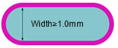
Figure 7. Non-plated Slots Minimum Width
Plated Slotted Holes

Some components like the DC barrel power jack/connectors, audio connector and some micro USB connectors, have wide and thin pins. You can drill a big round hole for them, but sometimes it’s not practical (e.g. round holes usually use more spaces). For these components, slotted holes become necessary.
Currently, there is no built-in mechanism to handle slotted holes directly in EAGLE. But there’s a workaround: Draw the slotted holes in the Milling layer (46). And you’d better draw these things in the footprint editor, with zero width lines and arcs.

Figure 8. Slotted Holes in Milling Layer (46)
The minimum plated slot width is 0.65mm (25.6 mils), which is drawn with top and bottom copper pads, as illustrated in the figure below.

Figure 9. Slotted Holes Minimum Width
Plated slotted holes will also be merged into the outline layer in our CAM file (i.e. in the *.GKO file).
| Important | Just to be safe, you can write a special instruction in the remark area in our ordering system when you place the order, write like: "Please note: there are 3 plated slotted holes in this design". Our CAM engineer will sort them out from the "context" (like the annular ring and solder mask opening) when processing the files. |
Plated Drills and Non-plated Drills
They are merged into a single drill file (i.e. the .XLN file).
Comments on Silkscreen Layers
By default, our CAM jobs use the following layers for silkscreen.
Table 2. Layers for Silkscreen
| Layer | Silkscreen |
|---|---|
| 21 tPlace | Top Silkscreen |
| 25 tName | |
| 22 bPlace | Bottom Silkscreen |
| 26 bName |
Sometimes, you may have extra things for Silkscreen, for instance:
- Artwork designed in another graphics software, need to be imported, it’s better to put it on a separate layer.
- Logos (bitmap or vector).
- tValue/bValue for some cases.
- tDocu/bDocu for some cases.
Sometimes, you may don’t need Silkscreen at all.
For these special cases, you can add/remove those layers for Silkscreen output manually before your process the job. You can also save the modified CAM job to another file name for future use.
Comments on Gerber File Naming Conventions
By default, different EDA software uses different naming conventions for Gerber files. To make the fab process smoother, we use the Protel naming conventions as you may already notice.
With Protel naming, the layer information is encoded in file extensions.
Table 3. Gerber File Naming Conventions JLCPCB Prefers
| Extension | Description |
|---|---|
| GBL | Bottom Copper Layer |
| GBO | Bottom Silkscreen/Overlay |
| GBS | Bottom Solder Mask |
| GBP | Bottom Paste Mask |
| GTL | Top Copper Layer |
| GTO | Top Silkscreen/Overlay |
| GTS | Top Solder Mask |
| GTP | Top Paste Mask |
| GKO | Keep Out Layer(Board Outline) |
| G1,G2,etc. | Inner Copper Layer 1, 2, etc. |
| XLN | Excellon Drill File |
Inspect Files in a Gerber Viewer
Before uploading your Gerber files to our website for production, it’s highly recommended to cross-check the generated files with a 3rd-party Gerber Viewer.
When you are checking the file, please pay attention to the following items.
- Does the board outline exist?
- Is the board outline watertight(continuous/no gaps)?
- Do all inner cutouts and unplated slots show in the GKO layer correctly?
- Do all drilling holes shown and are aligned with other layers correctly?
- Are vias covered or exposed as per your design?
- And the Silkscreen, do they look good?
- etc.
If you find any issues, fix them and export the Gerber/Drill Files and check them in the Gerber viewer again.
There are some nice Gerber viewers, just use the one you feel handy.
- Gerbv
- tracespace view
- Reference gerber viewer from Ucamco

Figure 10. View the Files in Gerbv
Generating BOM and Centroid Files for SMT
If you need the SMT service from JLCPCB, the BOM and centroid files need to be generated as well. Follow this tutorial to generate BOM and CPL from Eagle CAD automatically.