Help Center
How to Generate Gerber files from EasyEDA
Last updated on Apr 24, 2025
When you finish your PCB in EasyEDA, you can output the Fabrication Files(gerber file) via: File > Generate PCB Fabrication File(Gerber) , or Fabrication > PCB Fabrication File(Gerber).

After clicking, will open the Gerber generate window:
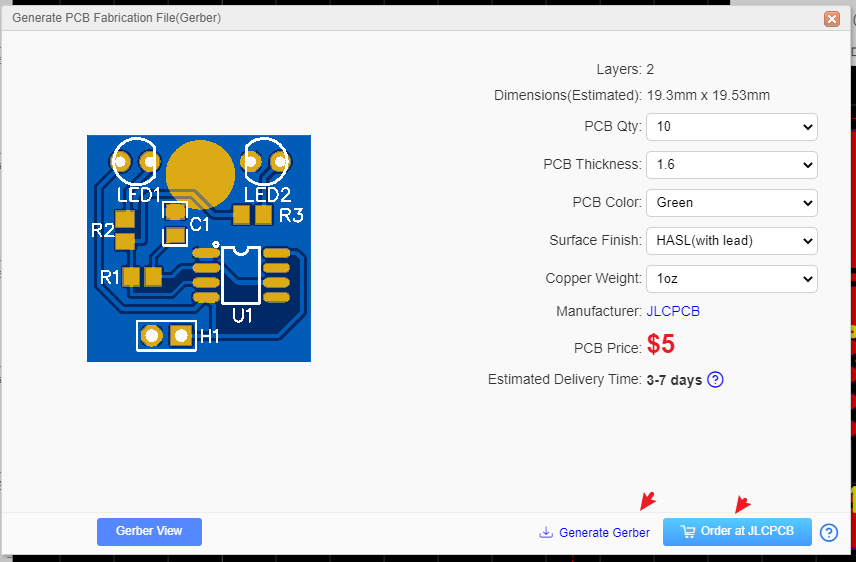
You can check the PCB price, and order the PCB at JLCPCB with one click. Or you can directly click the Generate Gerber to download the files.
Gerber file name
The generated Gerber file is a compressed zip file. After decompression, you can see the following files:
- Gerber_BoardOutlineLayer.GKO: PCB Border file. The PCB board factory cuts the shape of the board according to this document. The groove drawn by the EasyEDA, the solid region(Type: NPTH) is reflected in the border file after the Gerber is generated.
- Gerber_TopLayer.GTL: Top side copper layer.
- Gerber_BottomLayer.GBL: Bottom side copper layer.
- Gerber_Inner1.G1: Inner copper layer, signal type.
- Gerber_Inner2.GP2: Inner copper layer, plane type
- Gerber_TopSilkLayer.GTO: Top silkscreen.
- Gerber_BottomSilkLayer.GBO: Bottom silkscreen.
- Gerber_TopSolderMaskLayer.GTS: Top solder mask. The default board is covered with green oil, and the elements drawn on this layer correspond to the top layer’s area will not be covered with oil.
- Gerber_BottomSolderMaskLayer.GBS: Bottom solder mask. The default board is covered with green oil, and the elements drawn on this layer correspond to the bottom layer’s area will not be covered with oil.
- Drill_PTH_Through.DRL: Plated drill through hole layer. This document shows the location of the hole where the inner wall needs to be metallized. Old name: Gerber_Drill_PTH.DRL
- Drill_NPTH_Through.DRL: Non-Plated drill through hole layer. This document shows the location of the hole where the inner wall don’t need to be metallized. Old name: Gerber_Drill_NPTH.DRL
- Gerber_TopPasteMaskLayer.GTP: Top Paste Mask, for the stencil.
- Gerber_BottomPasteMaskLayer.GBP: Bottom Paste Mask, for the stencil.
- Gerber_TopAssemblyLayer.GTA:Top Assembly, read only, doesn’t affect the PCB manufacture. Old name: ReadOnly.TopAssembly
- Gerber_BottomAssemblyLayer.GBA: Bottom Assembly, read only, doesn’t affect the PCB manufacture. Old name: ReadOnly.BottomAssembly
- Gerber_MechanicalLayer.GML: Record the information on the mechanical layer in the PCB design, and only use it for information recording. Old name: ReadOnly.Mechanical. For example: process parameters; V cut path etc.
- Gerber_DocumentLayer.GDL: The document layer. It is used to record the remark information of the PCB and does not participate in the manufacturing.
Notice:
- Before ordering the PCB, please check the gerber at the Gerber view.
- The Gerber files are generated by browser, please use the browser inner downloader to download!
- The coordinates of the Gerber file follow the canvas coordinates
- When exporting Gerber, the drill file coordinate format accuracy defaults to 3:3. When the PCB size is out of range, it automatically uses 4:2 format. If you view the Gerber as such as CAM350, found that the Drill hole has been offset the location, you can modify the drill coordinate format to fit the location