Is FR4 the Best Board Material for Your Design
12 min
- What Is FR4 Substrate Material?
- What are the properties of FR4 substrate?
- Standard Manufacturing Process of FR4 PCBs
- When FR4 is Not Enough: Material Selection Guide
- Tips for selecting the right FR4 material
- FAQs about FR4 Material in PCB Design
- Conclusion
Key Takeaways
- Best All-Rounder: Ideal balance of strength, insulation, and low cost for standard PCBs.
- Clear Limits: Poor heat dissipation (~0.3 W/m·K) and high loss for RF (>3 GHz).
- Alternatives: Use Rogers for RF, Aluminum for high heat, and FPC for flexibility.
- Selection Essentials: Pick High-Tg (170°C+) for lead-free reflow and custom stackups for impedance.
- JLCPCB Advantage: 1–32 layer FR4 boards with ±10% impedance control and 24h fast dispatch.
In the world of electronics and printed circuit board manufacturing, choosing the right substrate material for your design can mean the difference between success and failure. FR4 substrate, with its excellent mechanical strength, electrical insulation, and resistance to heat and chemicals, is widely used in the industry. In this article, we will explore the properties and advantages of FR4 substrate, its use in printed circuit boards, as well as some limitations and tips for selecting the right FR4 material.
What Is FR4 Substrate Material?
FR4 substrate stands for "flame retardant 4" which indicates that FR4 substrate is made to resist the propagation of flames and meets certain fire safety standards. FR4 flame-retardant devices are used where fire safety is a concern like in electronics or electrical systems and flame retardancy acts as an added safety where there is a risk of fire accidents. It is a type of substrate that is used in the making of electrical components and is widely used in the manufacturing of printed circuit boards. This type of substrate has fiberglass as one of its components which provides mechanical strength along with epoxy resin. The combination of the two materials acts as an insulating matrix. FR4 substrates provide excellent electrical insulation, mechanical strength and protection for the electrical components on the board. They are resistant to heat and chemicals which makes them suitable to be used in various applications. FR4 substrates are best known for their durability, and mechanical strength which provide the board with dimensional stability and resistance to chemicals and moisture. They are widely used because of their high performance and cost-effectiveness. They provide excellent electrical insulation which results in reduced risks of short circuits and increases reliable signal transmission. FR4 substrates can hold their shape under different conditions due to their dimensional stability, which acts as an essential part of the proper mounting of electrical components on the printed circuit boards. If you need high-quality FR4 PCBs for your designs, you can easily place an order on the JLCPCB platform. JLCPCB’s smart, highly automated manufacturing facilities ensure precision quality with industry-leading turn-around times—delivering standard 2-layer PCB prototypes in as fast as 24 hours.
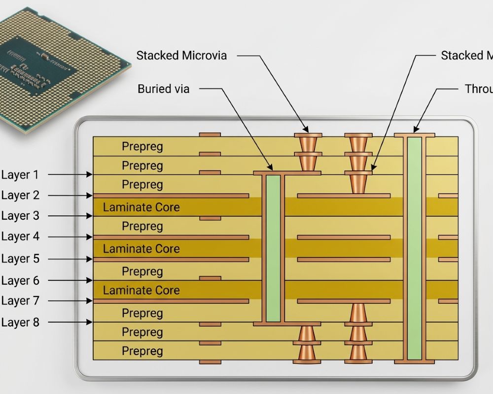
Understanding FR4 Internal Structure: Core vs. Prepreg (PP) in Multilayer PCBs
An FR4 PCB is rarely a single monolithic slice of material. In multilayer circuit boards (4 layers and above), FR4 exists in two primary physical forms:
1.FR4 Core (C-Stage Laminate): A fully cured rigid sheet of fiberglass impregnated with epoxy resin, clad with copper foil on both sides. It provides the central structural rigidity for the PCB.
2.Prepreg / PP (B-Stage Fiberglass ): A semi-cured fiberglass fabric impregnated with uncured resin. During high-temperature lamination, Prepreg melts, flows, fills the gaps between copper traces, and permanently bonds adjacent copper layers and Cores together.
Common FR4 Prepreg Types Used at JLCPCB :
7628 PP: Higher glass fabric thickness (~0.18mm), higher mechanical strength, lower resin content.
2116 PP: Medium thickness (~0.11mm), ideal balance for controlled impedance routing.
1080 PP: Thin PP (~0.07mm), high resin content, designed for high-density interconnect (HDI) and thin layer dielectric gaps.
JLCPCB FR4 Manufacturing Capabilities Overview
As a global leader in PCB prototype and mass production, JLCPCB provides industry-grade manufacturing capabilities tailored for FR4 designs:
| Capability Feature | JLCPCB Specification (JLCPCB 实际指标) |
|---|---|
| Layer Count | 1, 2, 4, 6, 8, ... up to 32 Layers |
| Board Thickness | 0.4mm, 0.6mm, 0.8mm, 1.0mm, 1.2mm, 1.6mm, 2.0mm, 3.2mm |
| Outer Copper Weight | 1oz / 2oz (2-layer boards support 2.5oz, 3.5oz, 4.5oz heavy copper) |
| Min. Trace Width / Space | 3.5mil / 3.5mil (0.09mm) for multilayer; 4mil / 4mil (0.1mm) for 1/2-layer |
| Min. Via Hole / Pad | 0.15mm hole / 0.25mm pad |
| Surface Finishes | HASL (Leaded), Lead-Free HASL, ENIG (1u"/2u"), OSP, Hard Gold |
| Turnaround Time | Prototype as fast as 24 Hours for 2-layer FR4 boards |
(Image credits: Jichangsheng Technology)
What are the properties of FR4 substrate?
It is the unique combination of mechanical, thermal, and electrical characteristics that makes FR4 the industry-standard substrate for printed circuit boards. Rather than viewing these properties in isolation, hardware engineers must evaluate them in relation to performance, heat management, and signal integrity. Below is a detailed technical analysis of the essential properties of FR4 substrate material.
Key Physical and Electrical Parameters
Understanding the performance thresholds of FR4 material is critical for robust hardware design. Below is a detailed technical parameter table representing standard FR4 substrates utilized in JLCPCB's fabrication facilities:
| arameter | Standard FR4 Value | High-Tg FR4 Value | Engineering Significance |
|---|---|---|---|
| Dielectric Constant (Dk @ 1MHz) | 4.2 – 4.8 | 4.2 – 4.6 | Determines signal propagation speed and impedance control. |
| Dissipation Factor (Df @ 1MHz) | ~0.02 | ~0.015 | Indicates signal loss; lower values are needed for high-frequency applications. |
| Glass Transition Temp. (Tg) | 130°C – 140°C | 170°C – 180°C | Temperature where resin softens; High-Tg handles lead-free reflow better. |
| Thermal Conductivity | ~0.3 W/m·K | ~0.4 W/m·K | Low thermal conductivity; requires thermal vias or heatsinks for high power. |
| Z-Axis CTE | 60–70 ppm/°C | 40–50 ppm/°C | Lower Z-axis expansion prevents plated through-hole (PTH) cracking during thermal shock. |
| Flammability Rating | UL94 V-0 | UL94 V-0 | Self-extinguishing within 10 seconds without flaming drips. |
Correction Note on Thermal & Environmental Properties:
Note that FR4 is inherently a thermal insulator (~0.3 W/m·K). For designs with high heat dissipation demands, thermal vias or metal-core boards (Aluminum PCBs) should be selected. Furthermore, environmental compliance relies on selecting RoHS/REACH-compliant Surface Finishes (such as Lead-Free HASL or ENIG) provided by JLCPCB.
Controlled Impedance for High-Speed Designs
In modern high-speed digital designs (e.g., USB 3.0, HDMI, Ethernet, Wi-Fi/Bluetooth antennas), FR4 traces behave as transmission lines rather than simple conductive paths. Maintaining controlled impedance (such as 50-ohm single-ended, 90-ohm or 100-ohm differential) is essential to prevent signal reflection, ringing, and electromagnetic interference (EMI).
Key factors governed by the FR4 substrate that impact impedance include:
Dielectric Constant (Dk): Standard FR4 exhibits a Dk of ~4.2-4.5 at 1 GHz. Consistent resin-to-glass ratio maintains stable Dk across the board.
Dielectric Height (H): The exact thickness of the Prepreg or Core layer between the signal trace and its reference plane.
Trace Geometry: Trace width (W) and copper thickness (T) directly determine the characteristic impedance.
JLCPCB provides a free online Impedance Calculator and Pre-designed Stackup Library, allowing engineers to select optimized FR4 stackups and automatically match required trace widths with tight +/- 10% impedance tolerances.
Standard Manufacturing Process of FR4 PCBs
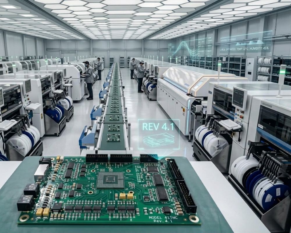
Transforming an FR4 substrate into a functional printed circuit board involves highly precise physical, chemical, and optical processes. Here is how JLCPCB manufactures high-quality FR4 PCBs:
Design & CAM Verification: CAD files (Gerber) are converted into production data and verified via Design for Manufacturing (DFM) checks.
Substrate Cutting & Pre-Baking : Large FR4 laminate sheets are cut to working sizes and pre-baked to eliminate internal stress and prevent warping.
Inner Layer Imaging & Etching : For multilayer boards, dry film photoresist is applied, UV exposed, and unneeded copper is etched away to form inner trace patterns.
Lamination : Core FR4 layers, Prepreg (PP), and copper foils are stacked and fused under high temperature and high pressure.
Precision CNC Drilling : Advanced CNC drilling machines create through-holes, blind vias, or buried vias according to design parameters.
PTH & Copper Plating : Chemical Deposition (PTH) coats non-conductive hole walls with copper, followed by electroplating to thicken copper traces and via walls.
Solder Mask Application : Liquid Photoimageable (LPI) solder mask is printed to protect copper traces from oxidation and prevent solder bridges.
Silkscreen Legend Printing: Component identifiers, logos, and test points are printed on top of the solder mask layer.
Surface Finishing : Finishes such as ENIG or Lead-Free HASL are applied to protect exposed copper pads and ensure optimal solderability.
Profiling & Electrical Testing : Boards are routed/V-cut to final dimensions and undergo 100% Flying Probe Testing or AOI inspection to guarantee zero defect.
When FR4 is Not Enough: Material Selection Guide
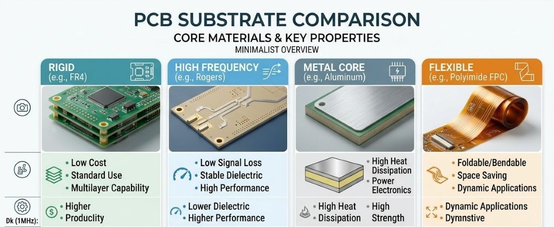
While FR4 is the most cost-effective substrate for general electronics, specific high-performance scenarios demand specialized materials available on the JLCPCB platform:
| Application Scenario | Limitation of FR4 | Recommended Alternative | Primary Advantage |
|---|---|---|---|
| High Frequency / RF (> 3–5 GHz) | High signal attenuation (Df ~0.02) and unstable Dk. | Rogers Laminates (e.g., RO4350B, RO4000) / PTFE | Very low loss tangent (Df ~0.0037) for stable RF performance. |
| High Power / Extreme Heat | Low thermal conductivity (~0.3 W/m·K) causes heat buildup. | Aluminum-Core PCBs / Copper-Core | High thermal conductivity (1.0–3.0 W/m·K) for LED & power modules. |
| Ultra-Thin & Dynamic Flexing | Rigid FR4 cannot bend; space constraints. | Flexible PCBs (FPC) / Rigid-Flex PCBs | Polyimide substrate allows 3D wiring and dynamic bending. |
| Extreme Thermal Cycling | High Z-axis CTE mismatch leads to via failure. | High-Tg FR4 (Tg170+) / Polyimide | Superior dimensional stability under thermal shock. |
Tips for selecting the right FR4 material
Here are some of the tips that will make you choose the right FR4 substrate.
THICKNESS: The thickness of the FR4 sheets determines whether you want more mechanical strength for your board made possible by thick sheets or you want a more compact design which will be possible by using thin FR4 sheets.
GLASS TRANSITION TEMPERATURE: Glass transition temperature is a very important property of an FR4 substrate This is the temperature where the substrate material transitions from a rigid to a flexible state. You should choose a substrate with a high enough glass transition temperature to avoid performance issues or other problems.
COPPER WEIGHT: Varying copper weight means different current carrying capacities for your design. Heavier (thicker) copper weight is used for better conductivity but heavier copper also makes the substrate more costly and also adds to the manufacturing challenges. Lighter copper weight enables less conductivity but the substrate gets cheaper.
FLAME RETARDANCY: Be on the lookout for those FR4 substrates that meet industry standards to comply with safety standards and regulations.
COST CONSIDERATION: Cost may vary depending on the different specifications of the substrate so be on the lookout for cheaper substrate if your work is not as professional and go for the pricey ones when your work is professional.
SUPPLIER SUPPORT: Make sure that you are in direct contact with the supplier who gave you your substrate because because they possess deep technological expertise regarding the compatibility of the substrate with your printed circuit board design.
FAQs about FR4 Material in PCB Design
Q: What is the difference between standard FR4 and High-Tg FR4?
The primary difference lies in their Glass Transition Temperature (Tg), where resin begins to soften. Standard FR4 typically has a Tg of 130°C–140°C, suitable for basic electronics and leaded soldering. High-Tg FR4 (Tg170°C+) offers superior thermal stability, lower Z-axis expansion, and better resistance to thermal shock, making it ideal for multilayer PCBs subjected to lead-free reflow soldering (peak 260°C) or operating in high-temperature environments.
Q: Is FR4 suitable for high-frequency or RF circuit designs?
Standard FR4 is generally limited to applications operating below 3–5 GHz due to its relatively high dielectric loss (Df ~0.02) and fluctuating dielectric constant (Dk). For high-frequency, RF, or microwave designs, specialized low-loss substrates such as Rogers laminates (e.g., RO4350B) or PTFE are recommended to minimize signal attenuation and ensure stable performance.
Q: Can FR4 effectively dissipate heat in high-power applications?
No, FR4 is inherently a poor thermal conductor with a thermal conductivity of only about 0.3 W/m·K. In high-power applications such as LED lighting or power converters, heat can be managed by adding arrays of thermal vias in the FR4 board or by switching to Aluminum-core metal PCBs, which offer thermal conductivities between 1.0 and 3.0 W/m·K.
Q: What is Controlled Impedance and how does FR4 support it?
Controlled Impedance ensures that PCB traces match target resistance values (e.g., 50-ohm single-ended or 90/100-ohm differential) to prevent signal reflections in high-speed circuits. It depends on the FR4 material's Dk, trace width, copper thickness, and dielectric thickness. JLCPCB provides standard FR4 stackup profiles and a free online Impedance Calculator to achieve precise +/- 10% impedance control.
Q: What FR4 manufacturing capabilities and delivery speeds does JLCPCB offer?
JLCPCB supports FR4 PCB designs ranging from 1 to 32 layers, with board thicknesses from 0.4mm to 3.2mm and various surface finishes including Lead-Free HASL, ENIG, and OSP. With advanced automated production facilities, JLCPCB can manufacture and ship standard 2-layer FR4 PCB prototypes in as fast as 24 hours.
Conclusion
FR4 substrate remains the industry standard for PCB manufacturing, offering an ideal balance of mechanical strength, electrical insulation, flame retardancy, and cost-effectiveness. It is the go-to choice for most consumer, industrial, and automotive electronic applications.
However, engineers must evaluate FR4's physical limits in demanding scenarios. For high-frequency RF, extreme heat dissipation, or flexible designs, specialized materials like Rogers, Aluminum-core, or Flex PCBs are better alternatives. By selecting the right board thickness, Tg rating, copper weight, and impedance profile, you can optimize both performance and manufacturability. Partnering with JLCPCB ensures high-precision FR4 fabrication, full IPC compliance, and rapid turnaround times—delivering standard prototypes in as fast as 24 hours.
Keep Learning
Choosing the Right PCB Solder Mask Material for Reliable PCBs
Key Takeaways Dual-Curing: UV defines openings; heat cures epoxy for durability. LPI vs. Coverlay: LPI for rigid boards; coverlay for flexible circuits. Color & Pitch: Green allows tighter dams (0.10 mm) than black/white (0.13 mm). Protection: Prevents solder bridges and seals copper from moisture. Cure Quality: Proper baking prevents mask peeling during plating and reflow. PCB solder mask material is a cured polymer film usually 10 to 30 µm (0.4 to 1.2 mil) thick. During reflow, it is the only barrie......
Safeguarding Circuit Boards Against Breakdown Voltage Failure
Key Takeaways Construction Matters: Breakdown voltage depends on stackup and defects, not raw material ratings. Stress Causes Failures: Heat and moisture degrade insulation over time, leading to field defects. Four Main Failure Modes: Insulation fails via internal voids, treeing, CAF growth, or surface tracking. Layout Design Fixes: Use dual prepregs, wider hole spacing, rounded trace corners, and isolation slots. Testing Split: Bare-board testing checks low-voltage net continuity, while hi-pot tests ......
Is FR4 the Best Board Material for Your Design
Key Takeaways Best All-Rounder: Ideal balance of strength, insulation, and low cost for standard PCBs. Clear Limits: Poor heat dissipation (~0.3 W/m·K) and high loss for RF (>3 GHz). Alternatives: Use Rogers for RF, Aluminum for high heat, and FPC for flexibility. Selection Essentials: Pick High-Tg (170°C+) for lead-free reflow and custom stackups for impedance. JLCPCB Advantage: 1–32 layer FR4 boards with ±10% impedance control and 24h fast dispatch. In the world of electronics and printed circuit bo......
Optimizing High-Voltage Circuit Safety with PCB Dielectric Strength
Key Takeaways Non-linear Scaling: Dielectric strength drops as thickness increases. Safety vs Signals: Dielectric strength ensures safety, while Dk controls signal speed. Material Selection: High-voltage safety depends on Tg, CTI, and moisture resistance. Spacing Rules: Clearance prevents air arcs, while creepage prevents surface tracking. Assembly Testing: Hi-pot testing requires finished assemblies, not bare boards. Dielectric strength is the number engineers quote to prove a board is safe at mains ......
How Copper Foil Shapes PCB Performance and Manufacturing Quality
Key Takeaways Weight: 1 oz copper ≈ 35 µm thickness; higher weight increases current capacity. Types: ED for standard rigid boards, RA for dynamic flex circuits. DFM & Loss: Smoother foil lowers RF loss; thicker foil requires wider trace spacing. The part of a PCB that actually carries the electrical signal is the copper foil. The strength comes from the glass weave, the resin is used to keep the layers together, and the solder mask is used to provide protection and separation of exposed copper. But w......
Why PCB Substrate Choice Matters More Than You Think
Key Takeaways Prevents Via Failures: Z-axis CTE expansion strains via barrels; right substrates prevent field failure. Specify Beyond FR-4: Name IPC-4101 sheets to guarantee proper Tg and lower thermal growth. Match Material to Need: Choose FR-4 for standard, Polyimide for flex, Aluminum for heat, and Rogers for >3 GHz. Use Real Fab Stackups: Prepreg weave alters Dk; compute impedance using real factory stackups. The PCB substrate is the one part of your board you never actually draw. You choose a thi......