
Design Guidelines for Flex PCB Panels on JLCPCB
9 min
- Requirements for Flex PCB Panels on JLCPCB
- Panelization Best Practices for High-Yield Manufacturing
- Panelization Best Practices for High-Yield Manufacturing
- FAQ about Design Guidelines for Flex PCB
- Conclusion
When placing orders for flexible PCBs (FPCs) on JLCPCB, several key points must be noted. Unlike rigid PCB panels, which often use mouse bites or V-cuts for depanelization, FPC panels require bridge (tab) connections.
Requirements for Flex PCB Panels on JLCPCB
FPC panelization differs significantly from rigid boards. Proper design ensures efficient manufacturing, high yield, and compatibility with SMT assembly. Key requirements are as follows:
- Internal Board Spacing: 2 mm (standard); preferably 3 mm when metal stiffeners are used. This extra space accommodates laser cutting and prevents deformation during handling.
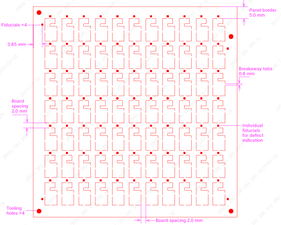
- Panel Borders (Process Edges): 5 mm on all sides. These areas must be covered with copper (for grounding/EMI protection), except for 1 mm clearance around fiducials and 0.5 mm around tooling holes.
- Fiducials and Tooling Holes: SMT fiducials: 1 mm diameter, centered 3.85 mm from panel edge. Tooling holes: 2 mm diameter. Place one fiducial and one tooling hole in each corner, offsetting those in one corner by at least 5 mm to indicate panel orientation and prevent 180° rotation errors.
- Connecting Tabs (Bridges): 0.7–1.0 mm wide. For stiffener-reinforced areas, use ~1.0 mm tabs and increase quantity to maintain panel stability during SMT reflow.
- Overall Panel Size: Recommended: 234 × 490 mm (optimal for production efficiency). Acceptable range: 70 × 70 mm minimum to ~250 × 500 mm maximum.
- For SMT Assembly Panels: Add one additional local fiducial next to each individual FPC unit. JLCPCB will paint over the fiducial of defective units to instruct the pick-and-place machine to skip them, reducing assembly costs.
FPCs with Metal Stiffeners: Require 0.8 mm slots (grooves) around each stiffener area for laser cutting/form ing, plus at least 3 mm board-to-board spacing.
| Parameter | Specification | Notes / Recommendations |
|---|---|---|
| Board Spacing | 2 mm (3 mm w/ stiffeners) | Prevents damage during laser depanelization |
| Process Edge | 5 mm all sides | Copper pour recommended |
| Fiducial | 1 mm dia., 3.85 mm from edge | Asymmetric placement for orientation |
| Tooling Hole | 2 mm dia. | One per corner + offset |
| Connecting Tab Width | 0.7–1.0 mm | Stronger/more tabs for heavy panels |
| Panel Size | 70×70 mm min; 234×490 mm recommended | Max ~250×500 mm |
Panelization Best Practices for High-Yield Manufacturing
Proper panelization is critical for flexible PCBs. The thin and flexible polyimide substrate is sensitive to mechanical stress and thermal changes, requiring special design considerations compared to rigid boards.FPC panels rely exclusively on laser-cut bridge tabs rather than V-cuts or mouse bites. This ensures structural integrity throughout fabrication, SMT processing, and final depanelization.
Key Panel Design Recommendations
- Process Edges (Borders): Maintain 5 mm wide borders on all four sides. These edges should be fully copper-poured (except clearances around fiducials and tooling holes) to provide mechanical stability and EMI shielding.
- Recommended Panel Size: Target 234 × 490 mm for optimal production efficiency and lowest cost. Acceptable range is 70 × 70 mm minimum to approximately 250 × 500 mm maximum.
- Material Utilization: Consistent spacing and standard panel dimensions help maximize boards per panel, reduce waste, and lower per-unit costs.
Fiducial and Tooling Hole Design for SMT Compatibility
Global fiducials and tooling holes ensure accurate alignment during fabrication and assembly. Follow these specifications:
1. Use 1 mm diameter SMT fiducials, centered 3.85 mm from the panel edge.
2. Add 2 mm diameter non-plated tooling holes in each corner.
3. Offset one corner’s fiducial and tooling hole by at least 5 mm to clearly indicate orientation and prevent 180° rotation errors.
4. For SMT assembly panels, place one additional local 1 mm fiducial next to each individual FPC unit. This allows JLCPCB to mark defective boards by painting over the fiducial, enabling automatic skip by pick-and-place machines.
Proper fiducial implementation significantly reduces misalignment risks, especially for fine-pitch components on flexible substrates prone to warping.
Panelization Best Practices for High-Yield Manufacturing
Proper panelization is critical for flexible PCBs. The thin and flexible polyimide substrate is sensitive to mechanical stress and thermal changes, requiring special design considerations compared to rigid boards.FPC panels rely exclusively on laser-cut bridge tabs rather than V-cuts or mouse bites. This design ensures structural integrity throughout fabrication, SMT processing, and final depanelization.
Key Panel Design Recommendations
- Process Edges (Borders): Maintain 5 mm wide borders on all four sides. These edges should be fully copper-poured (except 1 mm clearance around fiducials and 0.5 mm around tooling holes) to provide mechanical stability and EMI shielding.
- Recommended Panel Size: Target 234 × 490 mm for optimal production efficiency and lowest cost. Acceptable range is 70 × 70 mm minimum to approximately 250 × 500 mm maximum.
- Internal Board Spacing: Use 2 mm standard spacing, increasing to at least 3 mm when metal stiffeners are present.
Fiducial and Tooling Hole Design for SMT Compatibility
Global fiducials and tooling holes ensure accurate alignment during fabrication and assembly. Follow these specifications:
1. Use 1 mm diameter SMT fiducials, centered 3.85 mm from the panel edge.
2. Add 2 mm diameter non-plated tooling holes in each corner.
3. Offset one corner’s fiducial and tooling hole by at least 5 mm to clearly indicate orientation and prevent 180° rotation errors.
4. For SMT assembly panels, place one additional local 1 mm fiducial next to each individual FPC unit. JLCPCB can then mark defective boards by painting over the fiducial, allowing pick-and-place machines to automatically skip them.
Material Utilization and Cost Optimization Strategies
Effective panelization directly impacts material utilization rate and overall project cost. By maintaining consistent 2 mm inter-board spacing (3 mm with stiffeners) and utilizing the full recommended 234 × 490 mm panel area, designers can achieve significantly higher board counts per panel compared to irregular or undersized layouts. JLCPCB’s production bases are optimized for these standard dimensions, resulting in better economies of scale. Additional best practices include minimizing irregular board shapes where possible, grouping similar designs, and consulting JLCPCB’s third-party panelization service if self-panelization proves complex. These strategies reduce waste, lower per-unit pricing, and shorten lead times while maintaining full compliance with manufacturing tolerances.
FAQ about Design Guidelines for Flex PCB
Q: 1.Why can’t FPC panels use V-cuts or mouse bites?
FPC panels cannot use V-cuts or mouse bites because the thin and flexible polyimide substrate is highly sensitive to mechanical stress. These traditional depanelization methods can easily cause tearing, cracking, or deformation of the flex material. Instead, JLCPCB requires the exclusive use of laser-cut bridge tabs with a width of 0.7–1.0 mm to maintain structural integrity throughout the entire fabrication, SMT processing, and final separation stages.
Q: 2.What are the key requirements for panel borders?
Panel borders must be 5 mm wide on all four sides and should be fully covered with copper, except for the specified clearances around fiducials and tooling holes. These process edges provide essential mechanical support for automated handling equipment and contribute to EMI shielding. Proper implementation of the borders is crucial for panel stability during manufacturing and assembly.
Q: 3.What are the specifications for fiducials and tooling holes?
Global SMT fiducials should be 1 mm in diameter with their centers positioned 3.85 mm from the panel edge, while tooling holes should have a 2 mm diameter. One fiducial and one tooling hole must be placed in each corner of the panel, with those in one corner offset by at least 5 mm to clearly indicate orientation and prevent 180-degree rotation errors. For SMT assembly panels, an additional local 1 mm fiducial should be placed next to each individual FPC unit so that defective boards can be marked by painting over the fiducial.
Q: 4.What special rules apply to panels with metal stiffeners?
When using metal stiffeners, the board-to-board spacing in stiffened areas must be increased to at least 3 mm to accommodate the extra thickness and prevent deformation. Additionally, 0.8 mm wide clearance slots must be designed around each stiffener outline to enable precise laser cutting. Connecting tabs near stiffened regions should use the wider end of the specification (around 1.0 mm) and may require increased quantity to maintain panel stability during reflow soldering. These measures help prevent warping and ensure high assembly yield.
Q: 5.What is the recommended panel size and how to reduce cost?
The recommended panel size is 234 × 490 mm, with an acceptable range from a minimum of 70 × 70 mm to a maximum of approximately 250 × 500 mm. To optimize material utilization and reduce cost, designers should maintain consistent 2 mm (or 3 mm with stiffeners) board spacing, use regular board shapes, group similar designs together, and utilize the full standard panel area as much as possible. These practices maximize the number of boards per panel, minimize waste, lower per-unit pricing, and shorten lead times while remaining fully compliant with JLCPCB’s manufacturing capabilities.
Q: 6.What should I do for complex FPC panel designs?
For complex designs, especially those involving metal stiffeners or multiple different boards, it is best to strictly follow the requirements and best practices outlined in this document. After completing the Gerber files, upload them through JLCPCB’s online ordering system. The factory will perform a free panelization review and provide feedback if any adjustments are needed. Early consultation with JLCPCB support can effectively prevent potential manufacturing issues and ensure a smooth production process.
Conclusion
To achieve optimal performance and reliability in your flexible PCB designs, selecting high-quality materials and adhering to proper panelization guidelines are essential. JLCPCB works with leading global raw material suppliers to provide authentic A-grade polyimide substrates and consistently delivers high-quality flex circuits. With multiple intelligent production bases optimized for flexible PCB manufacturing, JLCPCB achieves excellent economies of scale while maintaining strict process control.
By following the panelization requirements outlined in this document — including 2 mm (or 3 mm with stiffeners) board spacing, 5 mm process edges, proper fiducials, tooling holes, and laser-cut tabs — designers can maximize production yield, reduce assembly defects, and ensure smooth SMT compatibility. These best practices not only improve manufacturing efficiency but also contribute to the overall success and long-term reliability of your flexible electronics projects.
Popular Articles
• 45 Must-Know Flex PCB Design Tips You Can't Afford to Miss!
• Choosing the Right Bend Radius for Durable Flexible PCBs
• FPC Design Rules: 13 Safety Distances You Can’t Ignore
• Mastering PCB Stiffeners: A Comprehensive Guide to Types, Applications, and Design Best Practices for Flexible Circuits
• How Flex Coverlay Protects and Enhances Flexible PCB Durability
Keep Learning
Flex PCB Manufacturing Process: From Prototyping To Mass Production
Flexible Printed Circuit Board commonly known as flex PCBs are a revolutionary step in modern electronics that offer compact, lightweight, dynamic and precise designs. Flex PCBs are designed to bend, twist, and fold, which rigid boards are incapable of. These characteristics have led to their widespread adoption in industries like wearable technology to consumer electronics to aerospace and medical technologies. With demands increasing day by day for miniaturized and ergonomic product designs, underst......
45 Must-Know Flex PCB Design Tips You Can't Afford to Miss!
Achieving perfection in product design requires a careful balance between meeting design requirements and manufacturing standards. However, when it comes to flex PCB (FPC) design, many engineers find themselves at a loss, unsure of where to begin. In this insightful guide, we will delve into 45 essential design guidelines for FPC. By the end, you'll have the knowledge and confidence to navigate the complexities of flex PCB design. Outline and Drilling 1. The minimum distance from through-holes to the ......
Choosing the Right Bend Radius for Durable Flexible PCBs
Key Takeaways Mastering the bend radius is essential for reliable flexible PCB design. Following IPC-2223 guidelines, maintain a minimum of 6× total thickness for static bends and 100× for dynamic applications, while using thinner RA copper, adhesiveless polyimide, staggered traces, and cross-hatched patterns in flex zones. Proper material selection, layer stackup optimization, and adequate clearance from stiffeners can dramatically extend flex life and prevent premature trace cracking or delamination......
FPC Connector Guide: Types, Pitch & Reliability
Key Takeaways Choosing the right FPC connector is critical for reliable flexible electronic designs. Connector type, pitch, pin count, stiffener thickness, and PCB layout all affect signal integrity and mechanical durability. By understanding FPC connector selection and design considerations, engineers can reduce connection failures and achieve reliable assembly results with JLCPCB. As you know, the electronics world is getting smaller; nowadays, the devices need to be thin and light. All the parts sh......
Flex PCB Design Guide: Preventing Mechanical Failures
Key Takeaways Reliable flex PCB design requires more than electrical performance. Proper bend radius control, trace routing, via placement, stiffener selection, and DFM considerations are essential to prevent mechanical failures such as copper cracking and delamination. By following proven flexible PCB design practices, engineers can improve durability and achieve reliable production results with JLCPCB. Ever wonder how the circuit in a foldable phone, fitness tracker, or camera module manages to rema......
Flex PCB Prototyping Guide: Materials & Design Tips
Key Takeaways A reliable flex PCB prototype requires more than just a working circuit. Material selection, bend radius control, copper design, panelization, and stiffener choices directly impact flexibility, durability, and manufacturing success. By following proper flexible PCB prototyping practices, engineers can reduce design risks and smoothly transition from prototypes to production with JLCPCB. Ever wonder how the circuit in a smartwatch, a foldable phone, or a camera module can take the shape? ......