


- Manufacturer
- MFR.Part #
- FI-RE51S-VF-R1300
- JLCPCB Part #
- C2886146
- Package
- SMD,P=0.5mm
- Description
- -40℃~+80℃ 0.5mm 1 1x51P 51 800mA IDC Header Surface Mount,Vertical SMD,P=0.5mm IDC Connectors ROHS
- EasyEDA Libraries
- ECCN
- EAR99
- Datasheet
- Source
- JLCPCB
- Assembly Type
- SMT Assembly
- PCBA Type
- Economic and Standard
- MSL Level
- MSL 1
Note: The purchased components are stored in your JLCPCB parts library for future PCBA orders only, and cannot be shipped separately.
| Attributes | Value | |
|---|---|---|
| Category | Connectors/IDC Connectors | |
| Manufacturer | JAE Electronics | |
| Package | SMD,P=0.5mm | |
| Operating Temperature | -40℃~+80℃ | |
| Number of Positions or Pins | 1x51P | |
| Number of Rows | 1 | |
| Contact Plating | Gold | |
| Current Rating | 800mA | |
| Pitch | 0.5mm | |
| Contact Material | Copper alloy | |
| Connector Type | IDC Header | |
| Holder Type | Surface Mount,Vertical | |
| Height Above Board | 4.65mm | |
| Number of PINs Per Row | 51 |
* Images are for reference only
FI-RE51S-VF-R1300
Extended- Manufacturer
- MFR.Part #
- FI-RE51S-VF-R1300
- JLCPCB Part #
- C2886146
- Package
- SMD,P=0.5mm
- Description
- -40℃~+80℃ 0.5mm 1 1x51P 51 800mA IDC Header Surface Mount,Vertical SMD,P=0.5mm IDC Connectors ROHS
- EasyEDA Libraries
- ECCN
- EAR99
- Datasheet
- Source
- JLCPCB
- Assembly Type
- SMT Assembly
- PCBA Type
- Economic and Standard
- MSL Level
- MSL 1
Note: The purchased components are stored in your JLCPCB parts library for future PCBA orders only, and cannot be shipped separately.
* Images are for reference only
- Manufacturer
- MFR.Part #
- FI-RE51S-VF-R1300
- JLCPCB Part #
- C2886146
- Package
- SMD,P=0.5mm
- Description
- -40℃~+80℃ 0.5mm 1 1x51P 51 800mA IDC Header Surface Mount,Vertical SMD,P=0.5mm IDC Connectors ROHS
- EasyEDA Libraries
- ECCN
- EAR99
- Datasheet
- Source
- JLCPCB
- Assembly Type
- SMT Assembly
- PCBA Type
- Economic and Standard
- MSL Level
- MSL 1
Note: The purchased components are stored in your JLCPCB parts library for future PCBA orders only, and cannot be shipped separately.
FI-RE51S-VF-R1300 Specifications
FI-RE51S-VF-R1300 technical specifications, attributes, and parameters.
| Attributes | Value | |
|---|---|---|
| Category | Connectors/IDC Connectors | |
| Manufacturer | JAE Electronics | |
| Package | SMD,P=0.5mm | |
| Operating Temperature | -40℃~+80℃ | |
| Number of Positions or Pins | 1x51P | |
| Number of Rows | 1 | |
| Contact Plating | Gold | |
| Current Rating | 800mA | |
| Pitch | 0.5mm | |
| Contact Material | Copper alloy | |
| Connector Type | IDC Header | |
| Holder Type | Surface Mount,Vertical | |
| Height Above Board | 4.65mm | |
| Number of PINs Per Row | 51 |
PCB Assembly Tips
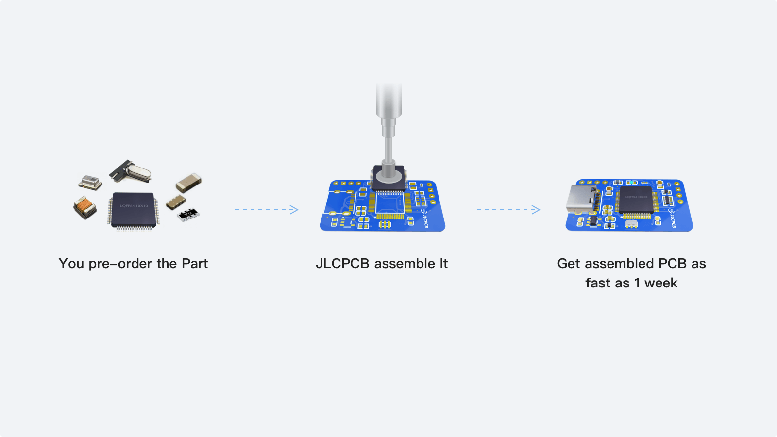
From components to fully assembled PCBs. JLCPCB supports PCB assembly for the FI-RE51S-VF-R1300. Sign up to receive and start your assembly today →
- 1
Step 1 - Pre-order the parts you need from JLCPCB.
- 2
Step 2 - Place a PCBA order to have those parts assembled onto your boards.
- 3
Step 3 - JLCPCB manufactures and assembles your boards in as fast as 3 days.
FI-RE51S-VF-R1300 Documents
FI-RE51S-VF-R1300 datasheets or manufacturer documentation.
Datasheet: FI-RE51S-VF-R1300 Datasheet (PDF)
FI-RE51S-VF-R1300 Schematic Symbol & PCB Footprint
The FI-RE51S-VF-R1300 schematic symbol and PCB footprint are available in the EasyEDA PCB design tool.