
YFW2309
- Manufacturer
- MFR.Part #
- YFW2309
- JLCPCB Part #
- C50326972
- Package
- SOT-23
- Description
- -55℃~+150℃ 1 P-Channel 1.56W 1.5V 145mΩ@10V、172mΩ@4.5V 20pF 2A 35pF 425pF 60V 8.2nC P-Channel SOT-23 MOSFETs ROHS
- EasyEDA Libraries
- ECCN
- -
- Source
- JLCPCB
- Assembly Type
- Wave Soldering
- PCBA Type
- Economic and Standard
- MSL Level
- MSL 1
Note: The purchased components are stored in your JLCPCB parts library for future PCBA orders only, and cannot be shipped separately.
| Attributes | Value | |
|---|---|---|
| Category | Transistors/Thyristors/MOSFETs | |
| Manufacturer | YFW | |
| Package | SOT-23 | |
| Operating Temperature | -55℃~+150℃ | |
| Input Capacitance(Ciss) | 425pF | |
| Type | P-Channel | |
| Number | 1 P-Channel | |
| Gate Threshold Voltage (Vgs(th)) | 1.5V | |
| Gate Charge(Qg) | 8.2nC | |
| Reverse Transfer Capacitance (Crss@Vds) | 20pF | |
| Current - Continuous Drain(Id) | 2A | |
| Drain to Source Voltage | 60V | |
| Output Capacitance(Coss) | 35pF | |
| Pd - Power Dissipation | 1.56W | |
| RDS(on) | 145mΩ@10V、172mΩ@4.5V |
* Images are for reference only
YFW2309
Extended- Manufacturer
- MFR.Part #
- YFW2309
- JLCPCB Part #
- C50326972
- Package
- SOT-23
- Description
- -55℃~+150℃ 1 P-Channel 1.56W 1.5V 145mΩ@10V、172mΩ@4.5V 20pF 2A 35pF 425pF 60V 8.2nC P-Channel SOT-23 MOSFETs ROHS
- EasyEDA Libraries
- ECCN
- -
- Source
- JLCPCB
- Assembly Type
- Wave Soldering
- PCBA Type
- Economic and Standard
- MSL Level
- MSL 1
Note: The purchased components are stored in your JLCPCB parts library for future PCBA orders only, and cannot be shipped separately.
YFW2309 Specifications
YFW2309 technical specifications, attributes, and parameters.
| Attributes | Value | |
|---|---|---|
| Category | Transistors/Thyristors/MOSFETs | |
| Manufacturer | YFW | |
| Package | SOT-23 | |
| Operating Temperature | -55℃~+150℃ | |
| Input Capacitance(Ciss) | 425pF | |
| Type | P-Channel | |
| Number | 1 P-Channel | |
| Gate Threshold Voltage (Vgs(th)) | 1.5V | |
| Gate Charge(Qg) | 8.2nC | |
| Reverse Transfer Capacitance (Crss@Vds) | 20pF | |
| Current - Continuous Drain(Id) | 2A | |
| Drain to Source Voltage | 60V | |
| Output Capacitance(Coss) | 35pF | |
| Pd - Power Dissipation | 1.56W | |
| RDS(on) | 145mΩ@10V、172mΩ@4.5V |
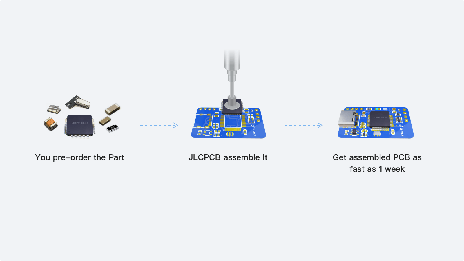
PCB Assembly Tips
From components to fully assembled PCBs. JLCPCB supports PCB assembly for the YFW2309. Sign up to receive and start your assembly today →
- 1
Step 1 - Pre-order the parts you need from JLCPCB.
- 2
Step 2 - Place a PCBA order to have those parts assembled onto your boards.
- 3
Step 3 - JLCPCB manufactures and assembles your boards in as fast as 3 days.
YFW2309 Schematic Symbol & PCB Footprint
The YFW2309 schematic symbol and PCB footprint are available in the EasyEDA PCB design tool.